SLVSEE9D April 2020 – April 2021 DRV8889-Q1
PRODUCTION DATA
- 1 Features
- 2 Applications
- 3 Description
- 4 Revision History
- 5 Pin Configuration and Functions
- 6 Specifications
-
7 Detailed Description
- 7.1 Overview
- 7.2 Functional Block Diagram
- 7.3
Feature Description
- 7.3.1 Stepper Motor Driver Current Ratings
- 7.3.2 PWM Motor Drivers
- 7.3.3 Microstepping Indexer
- 7.3.4 Controlling VREF with an MCU DAC
- 7.3.5 Current Regulation
- 7.3.6
Decay Modes
- 7.3.6.1 Slow Decay for Increasing and Decreasing Current
- 7.3.6.2 Slow Decay for Increasing Current, Mixed Decay for Decreasing Current
- 7.3.6.3 Mode 4: Slow Decay for Increasing Current, Fast Decay for Decreasing current
- 7.3.6.4 Mixed Decay for Increasing and Decreasing Current
- 7.3.6.5 Smart tune Dynamic Decay
- 7.3.6.6 Smart tune Ripple Control
- 7.3.7 Blanking Time
- 7.3.8 Charge Pump
- 7.3.9 Linear Voltage Regulators
- 7.3.10 Logic Level Pin Diagrams
- 7.3.11 Protection Circuits
- 7.4 Device Functional Modes
- 7.5 Programming
- 7.6 Register Maps
-
8 Application and Implementation
- 8.1 Application Information
- 8.2 Typical Application
- 9 Power Supply Recommendations
- 10Layout
- 11Device and Documentation Support
- 12Mechanical, Packaging, and Orderable Information
Package Options
Mechanical Data (Package|Pins)
Thermal pad, mechanical data (Package|Pins)
Orderable Information
8.2.4.2 PCB Types
Thermal analysis in this section is focused for the 2-layer and 4-layer PCB with two different copper thickness (1-oz and 2-oz) and six different copper areas (1-cm2, 2-cm2, 4-cm2, 8-cm2, 16-cm2 and 32-cm2), for both HTSSOP and VQFN packages.
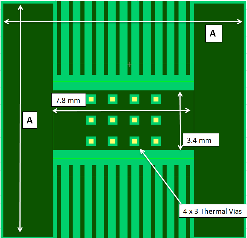
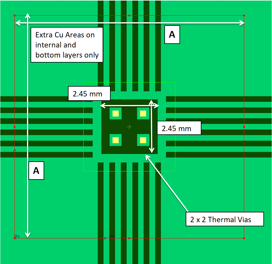
Figure 8-13 and Figure 8-14 show the top-layer which is applicable for both 2/4-layer PCB, for HTSSOP and VQFN packages respectively. The top-layer, mid-layer-1 and bottom-layer of the PCB is filled with ground plane, whereas, the mid-layer-2 is filled with power plane.
For the HTSSOP, 4 x 3 array of thermal vias with 300 µm drill diameter and 25 µm Cu plating were placed below the device package. For the VQFN, 2 x 2 array of thermal vias with 300 µm drill diameter and 25 µm Cu plating were placed below the device package. Thermal vias contacted top-layer, bottom-layer, and mid-layer-1 (ground plane) if applicable. The mid-layers and the bottom-layer were modeled with size A * A for both 2-layer and 4-layer designs. For the VQFN package, there was no copper on top layer outside of device land area.
The thickness of copper for different PCB layers in different PCB types is summarized in Table 8-3. The PCB dimension (A) for different PCB copper area is summarized in Table 8-4 for the HTSSOP package, and in Table 8-5 for the VQFN package.
| PCB Type | Copper Thickness | Top Layer | Bottom Layer | Mid-Layer 1 | Mid-Layer 2 |
|---|---|---|---|---|---|
| 2-Layer | 1-oz PCB | 1-oz | 1-oz | N/A | |
| 2-oz PCB | 2-oz | 2-oz | |||
| 4-Layer | 1-oz PCB | 1-oz | 1-oz | 1-oz | 1-oz |
| 2-oz PCB | 2-oz | 2-oz | 1-oz | 1-oz | |
 Figure 8-13 PCB - Top Layer (4/2-Layer PCB) for HTSSOP Package
 Figure 8-14 PCB - Top Layer (4/2-Layer PCB) for VQFN Package
| COPPER AREA (cm2) | DIMENSION (A) (mm) |
|---|---|
| 1 cm2 | 13.31 mm |
| 2 cm2 | 17.64 mm |
| 4 cm2 | 23.62 mm |
| 8 cm2 | 31.98 mm |
| 16 cm2 | 43.76 mm |
| 32 cm2 | 60.36 mm |
| COPPER AREA (cm2) | DIMENSION (A) (mm) |
|---|---|
| 1 cm2 | 10.00 mm |
| 2 cm2 | 14.14 mm |
| 4 cm2 | 20.00 mm |
| 8 cm2 | 28.28 mm |
| 16 cm2 | 40.00 mm |
| 32 cm2 | 56.57 mm |