SLVSEE9D April 2020 – April 2021 DRV8889-Q1
PRODUCTION DATA
- 1 Features
- 2 Applications
- 3 Description
- 4 Revision History
- 5 Pin Configuration and Functions
- 6 Specifications
-
7 Detailed Description
- 7.1 Overview
- 7.2 Functional Block Diagram
- 7.3
Feature Description
- 7.3.1 Stepper Motor Driver Current Ratings
- 7.3.2 PWM Motor Drivers
- 7.3.3 Microstepping Indexer
- 7.3.4 Controlling VREF with an MCU DAC
- 7.3.5 Current Regulation
- 7.3.6
Decay Modes
- 7.3.6.1 Slow Decay for Increasing and Decreasing Current
- 7.3.6.2 Slow Decay for Increasing Current, Mixed Decay for Decreasing Current
- 7.3.6.3 Mode 4: Slow Decay for Increasing Current, Fast Decay for Decreasing current
- 7.3.6.4 Mixed Decay for Increasing and Decreasing Current
- 7.3.6.5 Smart tune Dynamic Decay
- 7.3.6.6 Smart tune Ripple Control
- 7.3.7 Blanking Time
- 7.3.8 Charge Pump
- 7.3.9 Linear Voltage Regulators
- 7.3.10 Logic Level Pin Diagrams
- 7.3.11 Protection Circuits
- 7.4 Device Functional Modes
- 7.5 Programming
- 7.6 Register Maps
-
8 Application and Implementation
- 8.1 Application Information
- 8.2 Typical Application
- 9 Power Supply Recommendations
- 10Layout
- 11Device and Documentation Support
- 12Mechanical, Packaging, and Orderable Information
Package Options
Mechanical Data (Package|Pins)
Thermal pad, mechanical data (Package|Pins)
Orderable Information
7.3.5 Current Regulation
The current through the motor windings is regulated by a PWM current-regulation circuit. When an H-bridge is enabled, current rises through the winding at a rate dependent on the DC voltage, inductance of the winding, and the magnitude of the back EMF present. When the current hits the current regulation threshold, the bridge enters a decay mode for a period of time determined by the TOFF register setting and the selected decay mode to decrease the current. After the off-time expires, the bridge is re-enabled, starting another PWM cycle.
 Figure 7-5 Current Chopping Waveform
The PWM regulation current is set by a comparator which monitors the voltage across the current sense MOSFETs in parallel with the low-side power MOSFETs. The current sense MOSFETs are biased with a reference current that is the output of a current-mode sine-weighted DAC whose full-scale reference current is set by the voltage at the VREF pin. In addition, the TRQ_DAC register can further scale the reference current.
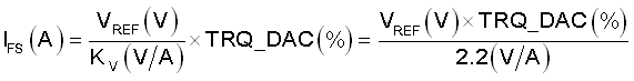
Use Equation 1 to calculate the full-scale regulation current.
The TRQ_DAC is adjusted via the SPI register. Table 7-6 lists the current scalar value for different inputs.
| TRQ_DAC | CURRENT SCALAR (TRQ) |
|---|---|
| 0000b | 100% |
| 0001b | 93.75% |
| 0010b | 87.5% |
| 0011b | 81.25% |
| 0100b | 75% |
| 0101b | 68.75% |
| 0110b | 62.5 |
| 0111b | 56.25% |
| 1000b | 50% |
| 1001b | 43.75% |
| 1010b | 37.5% |
| 1011b | 31.25% |
| 1100b | 25% |
| 1101b | 18.75% |
| 1110b | 12.5% |
| 1111b | 6.25% |