SBOS558D April   2011  – April 2025 INA200-Q1 , INA201-Q1 , INA202-Q1

PRODUCTION DATA  

  1.   1
  2. Features
  3. Applications
  4. Description
  5. Device Comparison
  6. Pin Configuration and Functions
  7. Specifications
    1. 6.1 Absolute Maximum Ratings
    2. 6.2 ESD Ratings
    3. 6.3 Recommended Operating Conditions
    4. 6.4 Thermal Information
    5. 6.5 Electrical Characteristics: Current-Shunt Monitor
    6. 6.6 Electrical Characteristics: Comparator
    7. 6.7 Electrical Characteristics: General
    8. 6.8 Typical Characteristics
  8. Parameter Measurement Information
    1. 7.1 Hysteresis
  9. Detailed Description
    1. 8.1 Overview
    2. 8.2 Functional Block Diagram
    3. 8.3 Feature Description
      1. 8.3.1 Comparator
      2. 8.3.2 Output Voltage Range
    4. 8.4 Device Functional Modes
  10. Application Information
    1. 9.1 Application Information
      1. 9.1.1 Basic Connections
      2. 9.1.2 Selecting RS
      3. 9.1.3 Input Filtering
      4. 9.1.4 Accuracy Variations as a Result of VSENSE and Common-Mode Voltage
        1. 9.1.4.1 Normal Case 1: VSENSE ≥ 20 mV, VCM ≥ VS
        2. 9.1.4.2 Normal Case 2: VSENSE ≥ 20 mV, VCM < VS
        3. 9.1.4.3 Low VSENSE Case 1: VSENSE < 20 mV, –16 V ≤ VCM < 0 V; and Low VSENSE Case 3: VSENSE < 20 mV, VS < VCM ≤ 80 V
        4. 9.1.4.4 Low VSENSE Case 2: VSENSE < 20 mV, 0 V ≤ VCM ≤ VS
      5. 9.1.5 Transient Protection
    2. 9.2 Typical Applications
      1. 9.2.1 Low-Side Switch Overcurrent Shutdown
        1. 9.2.1.1 Design Requirements
        2. 9.2.1.2 Detailed Design Procedure
        3. 9.2.1.3 Application Curves
      2. 9.2.2 High-Side Switch Overcurrent Shutdown
      3. 9.2.3 Bidirectional Overcurrent Comparator
    3. 9.3 Power Supply Recommendations
      1. 9.3.1 Output vs Supply Ramp Considerations
    4. 9.4 Layout
      1. 9.4.1 Layout Guidelines
      2. 9.4.2 Layout Example
  11. 10Device and Documentation Support
    1. 10.1 Receiving Notification of Documentation Updates
    2. 10.2 Support Resources
    3. 10.3 Trademarks
    4. 10.4 Electrostatic Discharge Caution
    5. 10.5 Glossary
  12. 11Revision History
  13. 12Mechanical, Packaging, and Orderable Information

Package Options

Mechanical Data (Package|Pins)
Thermal pad, mechanical data (Package|Pins)
Orderable Information

Basic Connections

Figure 9-1 shows the basic connections of the INA200-Q1, INA201-Q1, and INA202-Q1. Connect the input pins, VIN+ and VIN–, as close as possible to the shunt resistor to minimize any resistance in series with the shunt resistance.

Stability requires the use of power-supply bypass capacitors. Applications with noisy or high-impedance power supplies may require additional decoupling capacitors to reject power-supply noise. Connect bypass capacitors close to the device pins.
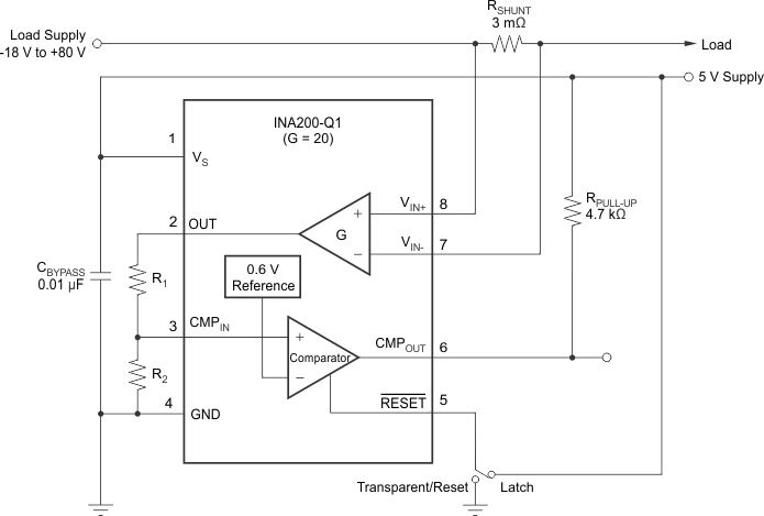
INA200-Q1 INA201-Q1 INA202-Q1 INA200-Q1 Basic ConnectionsFigure 9-1 INA200-Q1 Basic Connections