SBOS558D April   2011  – April 2025 INA200-Q1 , INA201-Q1 , INA202-Q1

PRODUCTION DATA  

  1.   1
  2. Features
  3. Applications
  4. Description
  5. Device Comparison
  6. Pin Configuration and Functions
  7. Specifications
    1. 6.1 Absolute Maximum Ratings
    2. 6.2 ESD Ratings
    3. 6.3 Recommended Operating Conditions
    4. 6.4 Thermal Information
    5. 6.5 Electrical Characteristics: Current-Shunt Monitor
    6. 6.6 Electrical Characteristics: Comparator
    7. 6.7 Electrical Characteristics: General
    8. 6.8 Typical Characteristics
  8. Parameter Measurement Information
    1. 7.1 Hysteresis
  9. Detailed Description
    1. 8.1 Overview
    2. 8.2 Functional Block Diagram
    3. 8.3 Feature Description
      1. 8.3.1 Comparator
      2. 8.3.2 Output Voltage Range
    4. 8.4 Device Functional Modes
  10. Application Information
    1. 9.1 Application Information
      1. 9.1.1 Basic Connections
      2. 9.1.2 Selecting RS
      3. 9.1.3 Input Filtering
      4. 9.1.4 Accuracy Variations as a Result of VSENSE and Common-Mode Voltage
        1. 9.1.4.1 Normal Case 1: VSENSE ≥ 20 mV, VCM ≥ VS
        2. 9.1.4.2 Normal Case 2: VSENSE ≥ 20 mV, VCM < VS
        3. 9.1.4.3 Low VSENSE Case 1: VSENSE < 20 mV, –16 V ≤ VCM < 0 V; and Low VSENSE Case 3: VSENSE < 20 mV, VS < VCM ≤ 80 V
        4. 9.1.4.4 Low VSENSE Case 2: VSENSE < 20 mV, 0 V ≤ VCM ≤ VS
      5. 9.1.5 Transient Protection
    2. 9.2 Typical Applications
      1. 9.2.1 Low-Side Switch Overcurrent Shutdown
        1. 9.2.1.1 Design Requirements
        2. 9.2.1.2 Detailed Design Procedure
        3. 9.2.1.3 Application Curves
      2. 9.2.2 High-Side Switch Overcurrent Shutdown
      3. 9.2.3 Bidirectional Overcurrent Comparator
    3. 9.3 Power Supply Recommendations
      1. 9.3.1 Output vs Supply Ramp Considerations
    4. 9.4 Layout
      1. 9.4.1 Layout Guidelines
      2. 9.4.2 Layout Example
  11. 10Device and Documentation Support
    1. 10.1 Receiving Notification of Documentation Updates
    2. 10.2 Support Resources
    3. 10.3 Trademarks
    4. 10.4 Electrostatic Discharge Caution
    5. 10.5 Glossary
  12. 11Revision History
  13. 12Mechanical, Packaging, and Orderable Information

Package Options

Mechanical Data (Package|Pins)
Thermal pad, mechanical data (Package|Pins)
Orderable Information

Normal Case 1: VSENSE ≥ 20 mV, VCM ≥ VS

This region of operation provides the highest accuracy. Here, use of a two-step method characterizes and measures the input offset voltage. First, Equation 2 determines the gain.
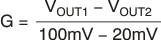
Equation 2. INA200-Q1 INA201-Q1 INA202-Q1

where:

VOUT1 = output voltage with VSENSE = 100 mV

VOUT2 = output voltage with VSENSE = 20 mV

Then the offset voltage is measured at VSENSE = 100 mV and referred to the input (RTI) of the current shunt monitor, as shown in Equation 3.

Equation 3. INA200-Q1 INA201-Q1 INA202-Q1

In the Typical Characteristics, Figure 6-6 (Output Error versus Common-Mode Voltage curve) shows the highest accuracy for the this region of operation. In this plot, VS = 12 V; for VCM ≥ 12 V, the output error is at its minimum. Using this case also creates the VSENSE ≥ 20 mV output specifications in the Electrical Characteristics: Current-Shunt Monitor table.