SNVSAL1C December 2017 – June 2021 LP87702-Q1
PRODUCTION DATA
- 1 Features
- 2 Applications
- 3 Description
- 4 Revision History
- 5 Description (continued)
- 6 Pin Configuration and Functions
- 7 Specifications
-
8 Detailed Description
- 8.1 Overview
- 8.2 Functional Block Diagram
- 8.3
Feature Descriptions
- 8.3.1 Step-Down DC/DC Converters
- 8.3.2 Boost Converter
- 8.3.3 Spread-Spectrum Mode
- 8.3.4 Sync Clock Functionality
- 8.3.5 Power-Up
- 8.3.6 Buck and Boost Control
- 8.3.7 Enable and Disable Sequences
- 8.3.8 Window Watchdog
- 8.3.9 Device Reset Scenarios
- 8.3.10 Diagnostics and Protection Features
- 8.3.11 OTP Error Correction
- 8.3.12 Operation of GPO Signals
- 8.3.13 Digital Signal Filtering
- 8.4 Device Functional Modes
- 8.5 Programming
- 8.6 Register Maps
- 9 Application and Implementation
- 10Power Supply Recommendations
- 11Layout
- 12Device and Documentation Support
- 13Mechanical, Packaging, and Orderable Information
Package Options
Mechanical Data (Package|Pins)
- RHB|32
Thermal pad, mechanical data (Package|Pins)
- RHB|32
Orderable Information
8.3.6.1 Enabling and Disabling Converters
The buck converters can be enabled when the device is in STANDBY or ACTIVE state. There are two ways to enable and disable the buck converters:
- Using BUCKx_EN bit in BUCKx_CTRL_1 register (BUCKx_EN_PIN_CTRL bit is 00 in BUCKx_CTRL_1 register)
- Using ENx control pin (BUCKx_EN bit is 1 in BUCKx_CTRL_1 register and BUCKx_EN_PIN_CTRL bit is not 00 in BUCKx_CTRL_1 register)
Similarly there are two ways to enable and disable the boost converter:
- Using BOOST_EN bit in BOOST_CTRL register (BOOST_EN_PIN_CTRL bit is 0 in BOOST_CTRL register)
- Using ENx control pin (BOOST_EN bit is 1 in BOOST_CTRL register and BOOST_EN_PIN_CTRL bit is not 00 in BOOST_CTRL register)
If the ENx control pin is used to enable and disable, then the delay from the control signal rising edge to start-up is set by BUCKx_STARTUP_DELAY[3:0] bits in BUCKx_DELAY register and BOOST_STARTUP_DELAY[3:0] bits in BOOST_DELAY register. The delay from falling edge of control signal to shutdown is set by BUCKx_SHUTDOWN_DELAY[3:0] bits in BUCKx_DELAY register and BOOST_SHUTDOWN_DELAY[3:0] bits in BOOST_DELAY register. The delays are valid only when ENx pin control is used, not when converters are enabled by I2C write to BUCKx_EN and BOOST_EN bits.
The control of the converters (with 0-ms delays) is shown in Table 8-3.
| BUCKx_EN / BOOST_EN | BUCKx_EN_PIN_CTRL / BOOST_EN_PIN_CTRL | EN1 PIN | EN2 PIN | EN3 PIN | BUCKx OUTPUT VOLTAGE / BOOST OUTPUT VOLTAGE | |
|---|---|---|---|---|---|---|
| Enable or disable control with BUCKx_EN/BOOST_EN bit | 0 | Don't Care | Don't Care | Don't Care | Don't Care | Disabled |
| 1 | 00 | Don't Care | Don't Care | Don't Care | BUCKx_VSET[7:0] / BOOST_VSET[1:0] | |
| Enable or disable control with EN1 pin | 1 | 01 | Low | Don't Care | Don't Care | Disabled |
| 1 | 01 | High | Don't Care | Don't Care | BUCKx_VSET[7:0] / BOOST_VSET[1:0] | |
| Enable/disable control with EN2 pin | 1 | 10 | Don't Care | Low | Don't Care | Disabled |
| 1 | 10 | Don't Care | High | Don't Care | BUCKx_VSET[7:0] / BOOST_VSET[1:0] | |
| Enable or disable control with EN3 pin | 1 | 11 | Don't Care | Don't Care | Low | Disabled |
| 1 | 11 | Don't Care | Don't Care | High | BUCKx_VSET[7:0] / BOOST_VSET[1:0] |
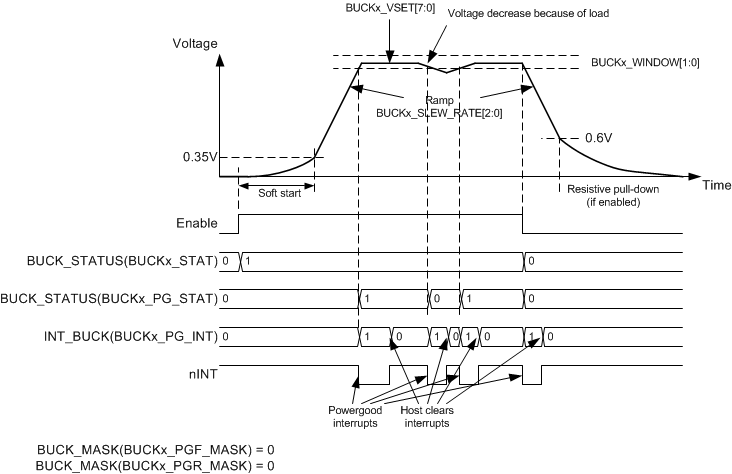
Figure 8-4 shows how the BUCKx converter is enabled by an ENx pin or by I2C write access. The soft-start circuit limits the in-rush current during start-up. The output voltage increase rate is typically 30 mV/μsec during soft start. The output voltage becomes slew-rate controlled when the output voltage rises to 0.35-V level. If there is a short circuit at the output and the output voltage does not increase above a 0.35-V level in 1 ms, the converter is disabled, and interrupt is set. When the output voltage rises above the undervoltage power-good threshold level the BUCKx_PG_INT interrupt flag in the INT_BUCK register is set.
Power-good thresholds are defined by BUCKx_WINDOW bits. A PGOOD_WINDOW bit in PGOOD_CTRL register sets the detection method for the valid buck output voltage, either undervoltage detection or undervoltage and overvoltage detection. The powergood interrupt flag can be masked using the BUCKx_PGR_MASK bit in the BUCK_MASK register when reaching the valid output voltage. The power-good interrupt flag can also be generated when the output voltage becomes invalid. The interrupt mask for invalid output voltage detection is set by BUCKx_PGF_MASK bit in BUCK_MASK register. When the window monitoring (under and overvoltage monitoring) is selected, the mask bits apply when voltage is crossing either threshold. A BUCKx_PG_STAT bit in BUCK_STAT register shows always the validity of the output voltage; '1' means valid, and '0' means invalid output voltage.
 Figure 8-4 Buck Converter Enable and Disable
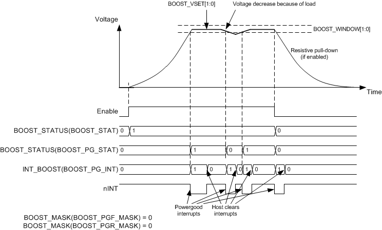
Figure 8-5 shows how the boost converter is enabled by an ENx pin or by I2C write access. The soft-start circuit limits the in-rush current during start-up. The output voltage increase rate is less than 100 mV/μsec during soft start. If there is a short circuit at the output and the output voltage does not reach the input voltage level in 1 ms, the converter is disabled, and the interrupt is set. When the output voltage reaches the power-good threshold level, the BOOST_PG_INT interrupt flag in INT_BOOST register is set.
Power-good thresholds are defined by BOOST_WINDOW bits. A PGOOD_WINDOW bit in PGOOD_CTRL register sets the detection method for the valid boost output voltage, either undervoltage detection or undervoltage and overvoltage detection. The power-good interrupt flag, when reaching valid output voltage, can be masked using BOOST_PGR_MASK bit in BOOST_MASK register. The power-good interrupt flag can also be generated when the output voltage becomes invalid. The interrupt mask for invalid output voltage detection is set by the BOOST_PGF_MASK bit in BOOST_MASK register. A BOOST_PG_STAT bit in the BOOST_STAT register always shows the validity of the output voltage; '1' means valid and '0' means invalid output voltage.
The ENx input pins have integrated pulldown resistors. The pulldown resistors are enabled by default and host can disable those with ENx_PD bits in CONFIG register.
 Figure 8-5 Boost Converter Enable and Disable