SLAS865F October 2014 – December 2021 MSP430FR4131 , MSP430FR4132 , MSP430FR4133
PRODUCTION DATA
- 1 Features
- 2 Applications
- 3 Description
- 4 Functional Block Diagram
- 5 Revision History
- 6 Device Comparison
- 7 Terminal Configuration and Functions
-
8 Specifications
- 8.1 Absolute Maximum Ratings
- 8.2 ESD Ratings
- 8.3 Recommended Operating Conditions
- 8.4 Active Mode Supply Current Into VCC Excluding External Current
- 8.5 Active Mode Supply Current Per MHz
- 8.6 Low-Power Mode LPM0 Supply Currents Into VCC Excluding External Current
- 8.7 Low-Power Mode LPM3, LPM4 Supply Currents (Into VCC) Excluding External Current
- 8.8 Low-Power Mode LPMx.5 Supply Currents (Into VCC) Excluding External Current
- 8.9 Typical Characteristics, Low-Power Mode Supply Currents
- 8.10 Current Consumption Per Module
- 8.11 Thermal Characteristics
- 8.12
Timing and Switching Characteristics
- 8.12.1 Power Supply Sequencing
- 8.12.2 Reset Timing
- 8.12.3 Clock Specifications
- 8.12.4 Digital I/Os
- 8.12.5 Timer_A
- 8.12.6
eUSCI
- 8.12.6.1 eUSCI (UART Mode) Operating Frequency
- 8.12.6.2 eUSCI (UART Mode) Switching Characteristics
- 8.12.6.3 eUSCI (SPI Master Mode) Operating Frequency
- 8.12.6.4 eUSCI (SPI Master Mode) Switching Characteristics
- 8.12.6.5 eUSCI (SPI Slave Mode) Switching Characteristics
- 8.12.6.6 eUSCI (I2C Mode) Switching Characteristics
- 8.12.7 ADC
- 8.12.8 LCD Controller
- 8.12.9 FRAM
- 8.12.10 Emulation and Debug
-
9 Detailed Description
- 9.1 CPU
- 9.2 Operating Modes
- 9.3 Interrupt Vector Addresses
- 9.4 Bootloader (BSL)
- 9.5 JTAG Standard Interface
- 9.6 Spy-Bi-Wire Interface (SBW)
- 9.7 FRAM
- 9.8 Memory Protection
- 9.9
Peripherals
- 9.9.1 Power Management Module (PMM) and On-Chip Reference Voltages
- 9.9.2 Clock System (CS) and Clock Distribution
- 9.9.3 General-Purpose Input/Output Port (I/O)
- 9.9.4 Watchdog Timer (WDT)
- 9.9.5 System Module (SYS)
- 9.9.6 Cyclic Redundancy Check (CRC)
- 9.9.7 Enhanced Universal Serial Communication Interface (eUSCI_A0, eUSCI_B0)
- 9.9.8 Timers (Timer0_A3, Timer1_A3)
- 9.9.9 Real-Time Clock (RTC) Counter
- 9.9.10 10-Bit Analog Digital Converter (ADC)
- 9.9.11 Liquid Crystal Display (LCD)
- 9.9.12 Embedded Emulation Module (EEM)
- 9.9.13
Input/Output Schematics
- 9.9.13.1 Port P1 Input/Output With Schmitt Trigger
- 9.9.13.2 Port P2 Input/Output With Schmitt Trigger
- 9.9.13.3 Port P3 Input/Output With Schmitt Trigger
- 9.9.13.4 Port P4.0 Input/Output With Schmitt Trigger
- 9.9.13.5 Port P4.1 and P4.2 Input/Output With Schmitt Trigger
- 9.9.13.6 Port 4.3, P4.4, P4.5, P4.6, and P4.7 Input/Output With Schmitt Trigger
- 9.9.13.7 Port P5.0, P5.1, P5.2, and P5.3 Input/Output With Schmitt Trigger
- 9.9.13.8 Port P5.4, P5.5, P5.6, and P5.7 Input/Output With Schmitt Trigger
- 9.9.13.9 Port P6 Input/Output With Schmitt Trigger
- 9.9.13.10 Port P7 Input/Output With Schmitt Trigger
- 9.9.13.11 Port P8.0 and P8.1 Input/Output With Schmitt Trigger
- 9.9.13.12 Port P8.2 and P8.3 Input/Output With Schmitt Trigger
- 9.10 Device Descriptors (TLV)
- 9.11 Memory
- 9.12 Identification
- 10Applications, Implementation, and Layout
- 11Device and Documentation Support
- 12Mechanical, Packaging, and Orderable Information
Package Options
Mechanical Data (Package|Pins)
Thermal pad, mechanical data (Package|Pins)
Orderable Information
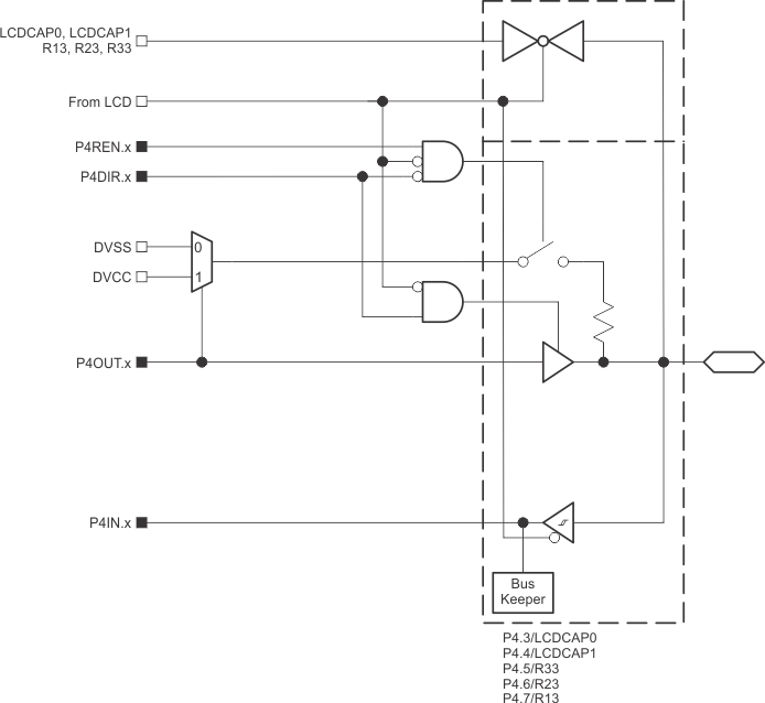
9.9.13.6 Port 4.3, P4.4, P4.5, P4.6, and P4.7 Input/Output With Schmitt Trigger
Figure 9-8 shows the port schematic. Table 9-19 summarizes the selection of the pin functions.
 Figure 9-8 Port 4.3, P4.4, P4.5, P4.6, and P4.7 Input/Output With Schmitt Trigger
Table 9-19 Port P4.3, P4.4, P4.5, P4.6, and P4.7 Pin Functions
| PIN NAME (P4.x) | x | FUNCTION | CONTROL BITS AND SIGNALS(1) | |
|---|---|---|---|---|
| P4DIR.x | LCDPCTL(2) | |||
| P4.3/LCDCAP0 | 3 | P4.3 (I/O) | I: 0; O: 1 | X |
| LCDCAP0 | X | 1 | ||
| P4.4/LCDCAP1 | 4 | P4.4 (I/O) | I: 0; O: 1 | 0 |
| LCDCAP1 | X | 1 | ||
| P4.5/R33 | 5 | P4.5 (I/O) | I: 0; O: 1 | 0 |
| R33 | X | 1 | ||
| P4.6/R23 | 6 | P4.6 (I/O) | I: 0; O: 1 | 0 |
| R23 | X | 1 | ||
| P4.7/R13 | 7 | P4.7 (I/O) | I: 0; O: 1 | 0 |
| R13 | X | 1 | ||
(1) X= don't care
(2) Setting the LCDPCTL bit in SYSCFG2 register will disable both the output driver and input Schmitt trigger to prevent leakage when analog signals are applied.