SBOS263H October 2002 – December 2024 OPA830
PRODUCTION DATA
- 1
- 1 Features
- 2 Applications
- 3 Description
- 4 Device Comparison Table
- 5 Pin Configurations
-
6 Specifications
- 6.1 Absolute Maximum Ratings
- 6.2 ESD Ratings
- 6.3 Recommended Operating Conditions
- 6.4 Thermal Information
- 6.5 Electrical Characteristics for D Package VS = ±5V
- 6.6 Electrical Characteristics for D Package VS = 5V
- 6.7 Electrical Characteristics for D Package VS = 3V
- 6.8 Electrical Characteristics for DBV Package VS = ±5V
- 6.9 Electrical Characteristics for DBV Package VS = 5V
- 6.10 Electrical Characteristics for DBV Package VS = 3V
- 6.11 Typical Characteristics: VS = ±5V
- 6.12 Typical Characteristics: VS = ±5V, Differential Configuration
- 6.13 Typical Characteristics: VS = 5V
- 6.14 Typical Characteristics: VS = 5V, Differential Configuration
- 6.15 Typical Characteristics: VS = 3V
- 6.16 Typical Characteristics: VS = 3V, Differential Configuration
- 7 Parameter Measurement Information
-
8 Application and Implementation
- 8.1
Application Information
- 8.1.1 Wideband Voltage-Feedback Operation
- 8.1.2 DC Level-Shifting
- 8.1.3 Optimizing Resistor Values
- 8.1.4 Bandwidth Versus Gain: Noninverting Operation
- 8.1.5 Inverting Amplifier Operation
- 8.1.6 Output Current and Voltages
- 8.1.7 Driving Capacitive Loads
- 8.1.8 Distortion Performance
- 8.1.9 Noise Performance
- 8.1.10 DC Accuracy and Offset Control
- 8.1.11 Thermal Analysis
- 8.2 Typical Applications
- 8.3 Layout
- 8.1
Application Information
- 9 Device and Documentation Support
- 10Revision History
- 11Mechanical, Packaging, and Orderable Information
Package Options
Refer to the PDF data sheet for device specific package drawings
Mechanical Data (Package|Pins)
- D|8
- DBV|5
Thermal pad, mechanical data (Package|Pins)
Orderable Information
8.1.9 Noise Performance
High slew rate, unity-gain stable, voltage-feedback op amps usually achieve a slew rate at the expense of a higher input noise voltage. The 9.2nV/√Hz input voltage noise for the OPA830, however, is much lower than comparable amplifiers. The input-referred voltage noise and the two input-referred current noise terms (2.8pA/√Hz) combine to give low output noise under a wide variety of operating conditions. Figure 8-6 shows the op amp noise analysis model with all the noise terms included. In this model, all noise terms are taken to be noise voltage or current density terms in either nV/√Hz or pA/√Hz.
 Figure 8-6 Noise Analysis Model
The total output spot noise voltage can be computed as the square root of the sum of all squared output noise voltage contributors. Figure 8-4 shows the general form for the output noise voltage using the terms shown in Figure 8-6:
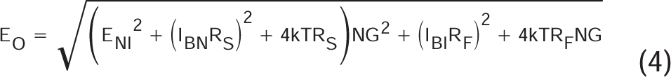
Dividing this expression by the noise gain (NG = (1 + RF / RG)) gives the equivalent input-referred spot noise voltage at the noninverting input, as shown in Figure 8-7:

Evaluating these two equations for the circuit and component values shown in Figure 8-1 gives a total output spot noise voltage of 19.3nV/√Hz and a total equivalent input spot noise voltage of 9.65nV/√Hz. This result includes the noise added by the resistors. This total input-referred spot noise voltage is not much greater than the 9.2nV/√Hz specification for the op amp voltage noise alone.