SLIS187C June   2021  – March 2022 TLC6A598

PRODUCTION DATA  

  1. Features
  2. Applications
  3. Description
  4. Revision History
  5. Pin Configuration and Functions
  6. Specifications
    1. 6.1 Absolute Maximum Ratings
    2. 6.2 ESD Ratings
    3. 6.3 Recommended Operating Conditions
    4. 6.4 Thermal Information
    5. 6.5 Electrical Characteristics
    6. 6.6 Timing Requirements
    7. 6.7 Timing Waveforms
    8. 6.8 Typical Characteristics
  7. Parameter Measurement Information
  8. Detailed Description
    1. 8.1 Overview
    2. 8.2 Functional Block Diagram
    3. 8.3 Feature Description
      1. 8.3.1 Serial-In Interface
      2. 8.3.2 Clear Registers
      3. 8.3.3 Output Channels
      4. 8.3.4 Register Clock
      5. 8.3.5 Cascade Through SER OUT
      6. 8.3.6 Output Control
      7. 8.3.7 Clamping Structure
      8. 8.3.8 Protection Functions
        1. 8.3.8.1 Overcurrent Protection
        2. 8.3.8.2 Output Detection
        3. 8.3.8.3 Serial Communication Error
        4. 8.3.8.4 Thermal Shutdown
      9. 8.3.9 Interface
        1. 8.3.9.1 Register Write
        2. 8.3.9.2 Register Read
        3. 8.3.9.3 Shift-Register Communication-Fault Detection
    4. 8.4 Device Functional Modes
      1. 8.4.1 Operation With VCC < 3 V
      2. 8.4.2 Operation With 5.5 V ≤ VCC ≤ 7 V
    5. 8.5 Register Maps
      1. 8.5.1 Configuration Register(Offset=0h)[reset=0h]
      2. 8.5.2 Fault Readback Register(Offset=1h)[reset=0h]
  9. Application and Implementation
    1. 9.1 Application Information
    2. 9.2 Typical Application 1
      1. 9.2.1 Design Requirements
      2. 9.2.2 Detailed Design Procedure
      3. 9.2.3 Application Curves
    3. 9.3 Typical Application 2
      1. 9.3.1 Design Requirements
      2. 9.3.2 Detailed Design Procedure
    4. 9.4 Typical Application 3
      1. 9.4.1 Design Requirements
      2. 9.4.2 Detailed Design Procedure
  10. 10Power Supply Recommendations
  11. 11Layout
    1. 11.1 Layout Guidelines
    2. 11.2 Layout Example
  12. 12Device and Documentation Support
    1. 12.1 Receiving Notification of Documentation Updates
    2. 12.2 Support Resources
    3. 12.3 Trademarks
    4. 12.4 Electrostatic Discharge Caution
    5. 12.5 Glossary
  13. 13Mechanical, Packaging, and Orderable Information

Package Options

Mechanical Data (Package|Pins)
Thermal pad, mechanical data (Package|Pins)
Orderable Information

Clamping Structure

When switching off inductive loads, the potential at pin OUT rises to VDS(CL) potential, because the inductance intends to continue driving the current. The clamping voltage is necessary to prevent destruction of the device. See Figure 8-1 for the clamping circuit principle. Nevertheless, the maximum allowed load inductance is limited.
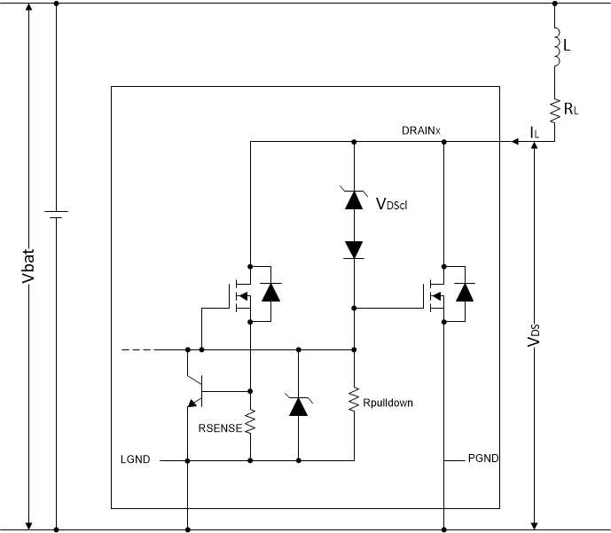
GUID-20200823-CA0I-LJCL-WZ7L-JRMTG3LLWDXQ-low.gif Figure 8-1 Output Clamp Implementation

During demagnetization of inductive loads, energy has to be dissipated in the TLC6A598. This energy can be calculated with Equation 1:

Equation 1. E= VDSCL×Vbat-VDSCLRL×ln1-RL×ILVbat-VDSCL+IL×LIL

The Equation 2 simplifies under the assumption of RL = 0:

Equation 2. E= 12×L×IL2×1-VbatVbat-VDSCL

The thermal design of the component limits the maximum energy, which is converted into heat.