SNIS241 September 2025 TMP461-EP
PRODUCTION DATA
- 1
- 1 Features
- 2 Applications
- 3 Description
- 4 Device Information
- 5 Pin Configuration and Functions
- 6 Specifications
- 7 Detailed Description
-
8 Register Map
- 8.1
Register Information
- 8.1.1 Pointer Register
- 8.1.2 Local and Remote Temperature Registers
- 8.1.3 Status Register
- 8.1.4 Configuration Register
- 8.1.5 Conversion Rate Register
- 8.1.6 One-Shot Start Register
- 8.1.7 Channel Enable Register
- 8.1.8 Consecutive ALERT Register
- 8.1.9 η-Factor Correction Register
- 8.1.10 Remote Temperature Offset Register
- 8.1.11 Manufacturer Identification Register
- 8.1
Register Information
- 9 Application and Implementation
- 10Device and Documentation Support
- 11Revision History
- 12Mechanical, Packaging, and Orderable Information
Package Options
Mechanical Data (Package|Pins)
- DGS|10
Thermal pad, mechanical data (Package|Pins)
Orderable Information
9.4.1 Layout Guidelines
Remote temperature sensing on the TMP461-EP device measures very small voltages using very low currents; therefore, noise at the device inputs must be minimized. Most applications using the TMP461-EP have high digital content, with several clocks and logic-level transitions that create a noisy environment. Layout must adhere to the following guidelines:
- Place the TMP461-EP device as close to the remote junction sensor as possible.
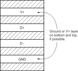
- Route the D+ and D– traces next to each other and shield them from adjacent signals through the use of ground guard traces, as shown in Figure 9-5. If a multilayer PCB is used, bury these traces between the ground or V+ planes to shield them from extrinsic noise sources. 5mil (0.127mm) PCB traces are recommended.
- Minimize additional thermocouple junctions caused by copper-to-solder connections. If these junctions are used, make the same number and approximate locations of copper-to-solder connections in both the D+ and D– connections to cancel any thermocouple effects.
- Use a 0.1μF local bypass capacitor directly between the V+ and GND of the TMP461-EP device. For optimum measurement performance, minimize filter capacitance between D+ and D– to 1000pF or less. This capacitance includes any cable capacitance between the remote temperature sensor and the TMP461-EP device.
- If the connection between the remote temperature sensor and the TMP461-EP device is less than 8in (20.32cm) long, use a twisted-wire pair connection. For lengths greater than 8 in, use a twisted, shielded pair with the shield grounded as close to the TMP461-EP device as possible. Leave the remote sensor connection end of the shield wire open to avoid ground loops and 60Hz pickup.
- Thoroughly clean and remove all flux residue in and around the pins of the TMP461-EP device to avoid temperature offset readings as a result of leakage paths between D+ and GND, or between D+ and V+.

NOTE: Use a minimum of 5mil (0.127mm) traces with 5mil spacing.
Figure 9-5 Suggested PCB Layer Cross-Section