SLUAAH6 November 2021 LM5110 , LM5111 , LM5112 , LM5112-Q1 , LM5114 , LM5134 , LMG1020 , LMG1025-Q1 , SM74101 , TPS2811 , TPS2813 , TPS2818-EP , TPS2819-EP , TPS2828 , TPS2829 , UCC27321 , UCC27322 , UCC27322-EP , UCC27322-Q1 , UCC27323 , UCC27324 , UCC27325 , UCC27332-Q1 , UCC27423 , UCC27423-Q1 , UCC27424 , UCC27424-EP , UCC27424-Q1 , UCC27425 , UCC27444 , UCC27444-Q1 , UCC27511 , UCC27511A , UCC27511A-Q1 , UCC27512 , UCC27512-EP , UCC27516 , UCC27517 , UCC27517A , UCC27517A-Q1 , UCC27518 , UCC27518A-Q1 , UCC27519 , UCC27519A-Q1 , UCC27523 , UCC27524 , UCC27524A , UCC27524A-Q1 , UCC27524A1-Q1 , UCC27525 , UCC27526 , UCC27527 , UCC27528 , UCC27531 , UCC27531-Q1 , UCC27532 , UCC27532-Q1 , UCC27533 , UCC27536 , UCC27537 , UCC27538 , UCC27611 , UCC27614 , UCC27614-Q1 , UCC27624 , UCC27624-Q1 , UCC37321 , UCC37322 , UCC37323 , UCC37324 , UCC37325 , UCC44273 , UCC57102 , UCC57102-Q1 , UCC57108 , UCC57108-Q1
4 Efficiency and Switching Performance
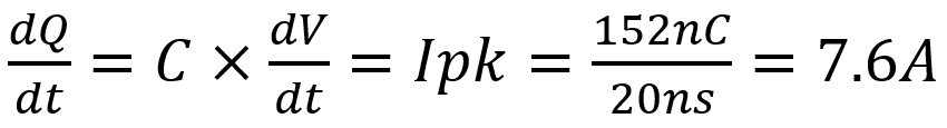
For example, if a MOSFET with gate charge of 156nC needs to be turned ON and OFF within 20ns, then the gate driver needs to supply 7.8 A of peak source and sink current, as shown in Equation 1.
UCC27614 is capable of delivering 10A even at junction temperature of 150C, which is confirmed in Figure 4-1. The high drive strength across temperature range allows the driver IC to consistently deliver fast and stable rise/fall times, ensuring minimum losses on the FETs regardless of the junction temperature.
Because power MOSFETs in these applications operate at high case temperatures, the gate driver needs to supply sufficient drive current regardless of temperature so that rise and fall times of the switching MOSFET can be minimized. Faster rise and fall times allows the MOSFET to be in the ohmic region for less time and get into the saturation region sooner, which results in less resistive losses in the transistor. The gate driver’s propagation delay should also be minimized, so that the dead time can be optimized, which results in lower losses and higher efficiency.
 Figure 4-1 Source and Sink Current at 12
V and 100nF Load Across Temperature
Figure 4-1 Source and Sink Current at 12
V and 100nF Load Across Temperature