SBAU315B July 2018 – March 2025 ADS9224R , ADS9234R
2.2.1 Input Signal Path
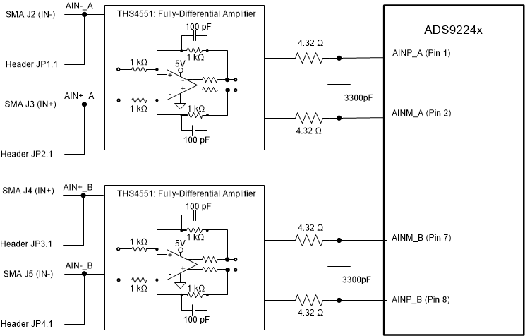
Figure 2-1 shows the signal path for the differential signal applied at the board inputs. The board input impedance is 1 kΩ. The overall signal-path bandwidth is limited to 1.5-MHz by the 1-kΩ resistor and 100-pF capacitor at the FDA feedback. The two THS4551 FDAs drive the ADS9224R differential inputs through an RC charge-kickback filter. These drivers provide a low dynamic impedance source at the ADC inputs at the full throughput of 3 MSPS.
 Figure 2-1 THS4551 Differential Input Driving Path
The ADS92x4REVM incorporates two THS4551 FDAs to drive the ADC inputs. The FDAs shift the signal to the appropriate common-mode voltage level. Figure 2-2 shows the fully-differential amplifier circuit. A differential input signal with a common-mode voltage of 0 V is applied to the inputs of the THS4551. The FDA establishes a fixed common-mode voltage at the ADC inputs using the FDA VOCM input pin. The ADS9224R incorporates a REF / 2 buffer output pin for setting the common-mode voltage. The ADS9224R REF / 2 output is connected to each THS4551 VOCM input pin. The THS4551 shifts the signal to the required common-mode voltage of REF / 2. Because of the THS4551 output swing specification to GND, either the input signals must be limited to a differential voltage of ±3.876 V amplitude in order to avoid saturating the amplifier output, or the negative supply must be driven below GND (in other words, –200 mV) to extend the output range.
 Figure 2-2 THS4551 Fully-Differential Amplifier Driver