SBOU024C august 2004 – july 2023 PGA309
- 1
- Read This First
-
1Introduction
- 1.1 PGA309 Functional Description
- 1.2 Sensor Error Adjustment Range
- 1.3 Gain Scaling
- 1.4 Offset Adjustment
- 1.5 Voltage Reference
- 1.6 Sensor Excitation and Linearization
- 1.7 ADC for Temperature Sensing
- 1.8 External EEPROM and Temperature Coefficients
- 1.9 Fault Monitor
- 1.10 Over-Scale and Under-Scale Limits
- 1.11 Power-Up and Normal Operation
- 1.12 Digital Interface
- 1.13 Pin Configuration
- 2Detailed Description
- 3Operating Modes
-
4Digital Interface
- 4.1 Description
- 4.2 Two-Wire Interface
- 4.3 One-Wire Interface
- 4.4 One-Wire Interface Timeout
- 4.5 One-Wire Interface Timing Considerations
- 4.6 Two-Wire Access to External EEPROM
- 4.7 One-Wire Interface Initiated Two-Wire EEPROM Transactions
- 4.8 PGA309 Stand-Alone Mode and Two-Wire Transactions
- 4.9 PGA309 Two-Wire Bus Master Operation and Bus Sharing Considerations
- 4.10 One-Wire Operation with PRG Connected to VOUT
- 4.11 Four-Wire Modules and One-Wire Interface (PRG)
- 5Application Background
-
6Register Descriptions
- 6.1 Internal Register Overview
- 6.2
Internal Register Map
- 6.2.1 Register 0: Temp ADC Output Register (Read Only, Address Pointer = 00000)
- 6.2.2 Register 1: Fine Offset Adjust (Zero DAC) Register (Read/Write, Address Pointer = 00001)
- 6.2.3 Register 2: Fine Gain Adjust (Gain DAC) Register (Read/Write, Address Pointer = 00010)
- 6.2.4 Register 3: Reference Control and Linearization Register (Read/Write, Address Pointer = 00011)
- 6.2.5 Register 4: PGA Coarse Offset Adjust and Gain Select/Output Amplifier Gain Select Register (Read/Write, Address Pointer = 00100)
- 6.2.6 Register 5: PGA Configuration and Over/Under-Scale Limit Register (Read/Write, Address Pointer = 00101)
- 6.2.7 Register 6: Temp ADC Control Register (Read/Write, Address Pointer = 00110)
- 6.2.8 Register 7: Output Enable Counter Control Register (Read/Write, Address Pointer = 00111)
- 6.2.9 Register 8: Alarm Status Register (Read Only, Address Pointer = 01000)
- A External EEPROM Example
- B Detailed Block Diagram
- C Glossary
- Revision History
3.2 EEPROM Content and Temperature Lookup Table Calculation
The PGA309 uses an industry standard, Two-Wire, external EEPROM (typically, a SOT23 package). A 1k-bit minimum EEPROM is needed if all 17 temperature coefficients are used. Larger EEPROMs may be used to provide additional user space for serial number, lot code, or other product data.
The 16-bit data words used by the PGA309 are stored in the external EEPROM, least significant 8-bit byte first, as shown in Figure 3-2.
 Figure 3-2 PGA309 Internal Registers Map to External EEPROM Addresses
Table 3-1 outlines the external EEPROM contents for a 1k−bit EEPROM. For a detailed External EEPROM Example refer to Appendix A.
The first part of the EEPROM (16 8-bit bytes), address location 1/0 through address location 15/14, contains the EEPROM Programmed Flag and the PGA309 configuration data for Registers 3, 4, 5, and 6. Included at the end of this section is Checksum1, at address location 15/14.
The second part of the EEPROM (108 8-bit bytes), address location 17/16 through address location 123/122, contains the temperature coefficient Lookup Table for the Zero DAC (Fine Offset Adjust) and Gain DAC (Fine Gain Adjust). There can be up to 17 temperature index values with corresponding scale factors for the Gain DAC and Zero DAC. The temperature values in the Lookup Table represent points on the piecewise linear curves that compensate for sensor span and offset temperature drifts. Each temperature value corresponds to respective slope factors for the Gain DAC and Zero DAC. The DAC values are linearly interpolated for a measured temperature that does not fall directly on a stored temperature value.
| EEPROM Address Location ‘1’ (Decimal) |
EEPROM Address Location ‘0’ (Decimal) |
Content (All data are stored as two 8-bit bytes) | |
|---|---|---|---|
| First Part | 1 | 0 | EEPROM Programmed Flag; 5449h = “TI” ascii |
| 3 | 2 | Not used, but include in Checksum1 calculation; available for user data. | |
| 5 | 4 | Not used, but include in the Checksum1 calculation; available for user data. | |
| 7 | 6 | Value for PGA309 Register 3, Reference Control and Linearization | |
| 9 | 8 | Value for PGA309 Register 4: PGA Coarse Offset and Gain/Output Amplifier Gain | |
| 11 | 10 | Value for PGA309 Register 5: PGA Configuration and Over/Under-Scale Limit | |
| 13 | 12 | Value for PGA309 Register 6: Temp ADC Control | |
| 15 | 14 | Checksum1= FFFFh − sum(hex values of location 1/0 thru 13/12) Checksum1 truncated above 16 bits | |
| Second Part | 17 | 16 | T0 (Temperature Index Value for Temp ≤ T0) |
| 19 | 18 | Z0 (Zero DAC Value for Temp ≤ T0) | |
| 21 | 20 | G0 (Gain DAC Value for Temp ≤ T0) | |
| 23 | 22 | T1 (Temperature Index Value T1) | |
| 25 | 24 | ZM1 (Zero DAC Multiplying Slope Factor for T1 ≤ Temp ≤ T0) | |
| 27 | 26 | GM1 (Gain DAC Multiplying Slope Factor for T1 ≤ Temp ≤ T0) | |
| ... | ... | ... | |
| ... | ... | ... | |
| ... | ... | ... | |
| 113 | 112 | T16 (Temperature Index Value T1) | |
| 115 | 114 | ZM16 (Zero DAC Multiplying Slope Factor for T15 ≤ Temp ≤ T16) | |
| 117 | 116 | GM16 (Gain DAC Multiplying Slope Factor for T15 ≤ Temp ≤ T16) | |
| 119 | 118 | TEND (End of Lookup Table → 7FFFh) | |
| 121 | 120 | ZMEND (End of Lookup Table; value ignored but included in Checksum2) | |
| 123 | 122 | GMEND (End of Lookup Table; value ignored but included in Checksum2) Checksum2 = FFFFh − sum(Hex values of location 17/16 thru 123/122) Checksum2 truncated above 16 bits | |
| 125 | 124 | Not used; available for user data | |
| 127 | 126 | Not used; available for user data |
T0, T1, T2 ... Tx (where x ≤ 16) are the temperature index values in the Lookup Table. These are output results from the Temp ADC. The values must be monotonically increasing from minimum to maximum for the Lookup Table to function correctly. Note that this does not necessarily correspond to increasing temperature. For example, if a diode voltage is being measured by the Temp ADC, its readings will be decreasing with temperature. However, the Lookup Table must still be built from minimum Temp ADC reading to the maximum Temp ADC reading. The data format for Tx is 16-bit data with a format dependent upon which Temp ADC mode is selected (see Section 6.2.7, Register 6: Temp ADC Control Register).
Z0 is the value of the Zero DAC setting for temperatures T0 and below. Z0 data format is unsigned 16-bit data. The equation for the Zero DAC value is:
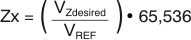
where 0 ≤ Zx ≤ 65535 (programmable range) and 0.1V ≤ Zero DAC ≤ VSA − 0.1V (analog limits).
G0 is the value of the Gain DAC setting for temperatures T0 and below. G0 data format is unsigned 16−bit data. The equation for the Gain DAC value is:
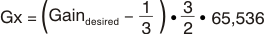
where 0.3333333 ≤ Gain DAC ≤ 0.9999898 and 0 ≤ Gx ≤ 65535.
ZM1, ZM2 … ZMi are multiplying slope factors for each piecewise linear segment for the Zero DAC adjustment. They are calculated based on the desired values Z1, Z2 … Zx (calculated same as Z0) of the Zero DAC for T1, T2 … Tx respectively. The equation for calculating the ZMi slope factors is:
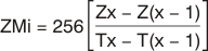
The ZMi scale factor of 256 is to format the decimal value for PGA309 internal binary arithmetic. These numbers are 16-bit, Twos Complement data format. See Table 3-2 for an example of the Lookup Table.
GM1, GM2 … GMi are multiplying slope factors for each piecewise linear segment for the Gain DAC adjustment. They are calculated based on the desired values G1, G2 … Gx (calculated the same as G0) of the Gain DAC for T1, T2, T3 …Tx, respectively. The equation for calculating the GMi slope factors is:
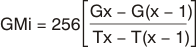
The GMi scale factor of 256 is to format the decimal value for PGA309 internal arithmetic. These numbers are 16-bit, Two’s-Complement data format.
The end of the Lookup Table is flagged by temperature index value TEND = 7FFFh in the temperature index data. The ZMEND value of this entry is ignored but is included in Checksum2. The ZMEND value should be set to zero. The GMEND value of this entry becomes Checksum2, the checksum for the second part of the EEPROM.
Example3-1 details the calculation of Lookup Table values and how the PGA309 lookup table linear interpolation algorithm works.