SBOU024C august 2004 – july 2023 PGA309
- 1
- Read This First
-
1Introduction
- 1.1 PGA309 Functional Description
- 1.2 Sensor Error Adjustment Range
- 1.3 Gain Scaling
- 1.4 Offset Adjustment
- 1.5 Voltage Reference
- 1.6 Sensor Excitation and Linearization
- 1.7 ADC for Temperature Sensing
- 1.8 External EEPROM and Temperature Coefficients
- 1.9 Fault Monitor
- 1.10 Over-Scale and Under-Scale Limits
- 1.11 Power-Up and Normal Operation
- 1.12 Digital Interface
- 1.13 Pin Configuration
- 2Detailed Description
- 3Operating Modes
-
4Digital Interface
- 4.1 Description
- 4.2 Two-Wire Interface
- 4.3 One-Wire Interface
- 4.4 One-Wire Interface Timeout
- 4.5 One-Wire Interface Timing Considerations
- 4.6 Two-Wire Access to External EEPROM
- 4.7 One-Wire Interface Initiated Two-Wire EEPROM Transactions
- 4.8 PGA309 Stand-Alone Mode and Two-Wire Transactions
- 4.9 PGA309 Two-Wire Bus Master Operation and Bus Sharing Considerations
- 4.10 One-Wire Operation with PRG Connected to VOUT
- 4.11 Four-Wire Modules and One-Wire Interface (PRG)
- 5Application Background
-
6Register Descriptions
- 6.1 Internal Register Overview
- 6.2
Internal Register Map
- 6.2.1 Register 0: Temp ADC Output Register (Read Only, Address Pointer = 00000)
- 6.2.2 Register 1: Fine Offset Adjust (Zero DAC) Register (Read/Write, Address Pointer = 00001)
- 6.2.3 Register 2: Fine Gain Adjust (Gain DAC) Register (Read/Write, Address Pointer = 00010)
- 6.2.4 Register 3: Reference Control and Linearization Register (Read/Write, Address Pointer = 00011)
- 6.2.5 Register 4: PGA Coarse Offset Adjust and Gain Select/Output Amplifier Gain Select Register (Read/Write, Address Pointer = 00100)
- 6.2.6 Register 5: PGA Configuration and Over/Under-Scale Limit Register (Read/Write, Address Pointer = 00101)
- 6.2.7 Register 6: Temp ADC Control Register (Read/Write, Address Pointer = 00110)
- 6.2.8 Register 7: Output Enable Counter Control Register (Read/Write, Address Pointer = 00111)
- 6.2.9 Register 8: Alarm Status Register (Read Only, Address Pointer = 01000)
- A External EEPROM Example
- B Detailed Block Diagram
- C Glossary
- Revision History
A.1 PGA309 External EEPROM Example
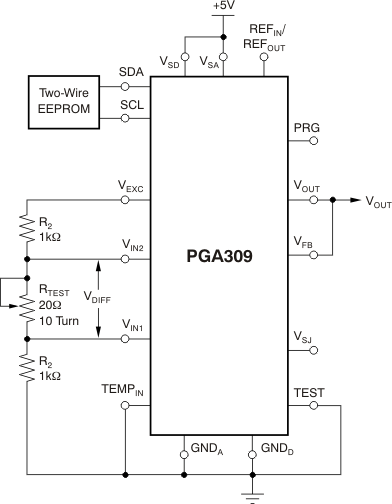
The PGA309 circuit configuration in Figure 7-1 is used in the PGA309EVM (Evaluation Module) to check proper functionality of the PGA309. Table 7-1 details the desired configuration for the PGA309. The Gain and Offset Scaling are shown in Example7-1. Figure 7-2 shows how the internal PGA309 16-bit data is mapped into the external EEPROM 8-bit address locations. The external EEPROM values are displayed in Table 7-2, which also details how Checksum1 and Checksum2 are computed for this example.
 Figure 7-1 PGA309 Circuit for External EEPROM Example
Table 7-1 PGA309 Configuration for External EEPROM Example
| Parameter | Desired Setting | Comments |
|---|---|---|
| VDIFF | 0V to 33.67mV | Adjust RTEST from 0Ω to 20Ω |
| VREF | 4.096V | Use Internal PGA309 Reference |
| VEXC | 3.4V | Use Linearization Circuit, Range 0 (KEXC = 0.83), Lin DAC = 0 |
| Coarse Offset | −3.277mV | |
| Front-End PGA Gain | 64 | |
| Gain DAC | 1 | |
| Output Amplifier Gain | 2.4 | |
| Zero DAC | 100mV | |
| Over-Scale | 3.876V | |
| Under-Scale | 0.245V | |
| VOUT Ideal | −0.263V to +4.908V | With Over-Scale and Under-Scale Disabled |
| VOUT Final | 0.245V to 3.876V | With Over-Scale and Under-Scale Enabled |
| Fault Detection | External Comparators | Enable |
| Fault Detect Polarity | Positive | |
| Internal Comparators | Disable | |
| Temperature ADC | Internal Mode | |
| Output Enable Counter | Set To All Zeroes | |
| EEPROM Temperature Coefficients | Set so all temperatures ≤ +128°C use same Gain DAC and Zero DAC settings |