SBOU024C august 2004 – july 2023 PGA309
- 1
- Read This First
-
1Introduction
- 1.1 PGA309 Functional Description
- 1.2 Sensor Error Adjustment Range
- 1.3 Gain Scaling
- 1.4 Offset Adjustment
- 1.5 Voltage Reference
- 1.6 Sensor Excitation and Linearization
- 1.7 ADC for Temperature Sensing
- 1.8 External EEPROM and Temperature Coefficients
- 1.9 Fault Monitor
- 1.10 Over-Scale and Under-Scale Limits
- 1.11 Power-Up and Normal Operation
- 1.12 Digital Interface
- 1.13 Pin Configuration
- 2Detailed Description
- 3Operating Modes
-
4Digital Interface
- 4.1 Description
- 4.2 Two-Wire Interface
- 4.3 One-Wire Interface
- 4.4 One-Wire Interface Timeout
- 4.5 One-Wire Interface Timing Considerations
- 4.6 Two-Wire Access to External EEPROM
- 4.7 One-Wire Interface Initiated Two-Wire EEPROM Transactions
- 4.8 PGA309 Stand-Alone Mode and Two-Wire Transactions
- 4.9 PGA309 Two-Wire Bus Master Operation and Bus Sharing Considerations
- 4.10 One-Wire Operation with PRG Connected to VOUT
- 4.11 Four-Wire Modules and One-Wire Interface (PRG)
- 5Application Background
-
6Register Descriptions
- 6.1 Internal Register Overview
- 6.2
Internal Register Map
- 6.2.1 Register 0: Temp ADC Output Register (Read Only, Address Pointer = 00000)
- 6.2.2 Register 1: Fine Offset Adjust (Zero DAC) Register (Read/Write, Address Pointer = 00001)
- 6.2.3 Register 2: Fine Gain Adjust (Gain DAC) Register (Read/Write, Address Pointer = 00010)
- 6.2.4 Register 3: Reference Control and Linearization Register (Read/Write, Address Pointer = 00011)
- 6.2.5 Register 4: PGA Coarse Offset Adjust and Gain Select/Output Amplifier Gain Select Register (Read/Write, Address Pointer = 00100)
- 6.2.6 Register 5: PGA Configuration and Over/Under-Scale Limit Register (Read/Write, Address Pointer = 00101)
- 6.2.7 Register 6: Temp ADC Control Register (Read/Write, Address Pointer = 00110)
- 6.2.8 Register 7: Output Enable Counter Control Register (Read/Write, Address Pointer = 00111)
- 6.2.9 Register 8: Alarm Status Register (Read Only, Address Pointer = 01000)
- A External EEPROM Example
- B Detailed Block Diagram
- C Glossary
- Revision History
4.3 One-Wire Interface
The PGA309 may be configured through a One-Wire UART-compatible interface (PRG pin). This interface also allows programming of the external industry-standard Two-Wire EEPROM device. There are six possible communication transactions. These transactions allow the internal register pointer to be updated, the external EEPROM pointer to be updated, internal registers to be read, internal registers to be written, EEPROM data to be read, and EEPROM data to be written. It is possible to connect the PRG pin, which uses the One-Wire interface, to the VOUT pin in true three-wire sensor module applications and still allow for digital programming.
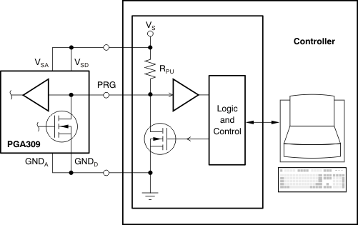
Each transaction consists of several bytes of data transfer. Each byte consists of 10 bit periods. The first bit is the start bit and is always zero. The PRG pin should always be high when no communication is in progress. The one-to-zero (high-to-low) transition of the PRG pin signals the start of a byte transfer and all timing information for the current byte is referenced to this transition. Bits 2 thru 9 are the eight data bits for the byte and are transferred least significant bit (LSB) first. The tenth bit is the stop bit and is always ‘1’. The recommended circuit implementation to interface to the PRG pin uses a pull-up resistor and/or pull-up current source with an open drain (or open collector) driver connected to the PRG pin. (The PRG pin is also an open drain output. The PRG pin may be driven high by the digital programmer (controller) during transmit from the controller, but some form of pull-up will be required to allow the signal to go high during a receive transaction, since the PGA309 can only pull the output low. Figure 4-5 shows a typical connection between the PGA309 PRG pin and the controller.
 Figure 4-5 Typical PGA309 PRG To Controller Connection
All communication transactions start with an initialization byte transmitted by the controller. This byte (55h) is used to sense the baud rate used for the communication transaction. The baud rate is sensed during the initialization byte of every transaction. This baud rate is used for the entire transaction. Each transaction may use a different baud rate if desired. Baud rates of 4800 to 38400 are supported. The second byte is a command byte transmitted by the controller.
There are six possible commands:
- Set PGA309 Register Address Pointer (01h)
- Set EEPROM Address Pointer (02h)
- Write PGA309 Register (04h)
- Write EEPROM (08h)
- Read PGA309 Register (10h)
- Read EEPROM (20h)
See Figure 4-6 for timing details of these transactions.
 Figure 4-6 One-Wire (PRG) Access to PGA309 and External EEPROM Timing
Data transfer occurs after the command byte. The number of bytes and direction of data transfer depend on the command byte.
For the Set PGA309 Register Address Pointer (01h) command, one additional byte is required to be transmitted by the controller. This is used to select the PGA309 internal register for the next PGA309 Write Register (04h) or PGA309 Read Register (10h) command. For the PGA309 Write Register command, two additional bytes are required to be transmitted by the controller. These two bytes, transmitted least significant byte first, are stored in the PGA309 internal register pointed to by the register address pointer. The addressed register will be updated with all 16 bits simultaneously at the completion of the transfer of the second byte. For the PGA309 Read Register (10h) command, two additional bytes are transmitted by the PGA309. The PGA309 waits for eight bit periods after the completion of the command byte before beginning transmission. This allows time for the controller to ensure that the PGA309 will be able to control the One-Wire interface. The first byte transmitted is the least significant byte of the register and the second byte is the most significant byte of the register.
For a One-Wire PGA309 sequence, the transactions may be repeated immediately one after the other, as shown in Figure 4-7. For a One-Wire PGA309 register read sequence, the transactions may be repeated after the data has been received from the PGA309, also shown in Figure 4-7.
 Figure 4-7 One-Wire Access to PGA309 Registers
For the Set EEPROM Address Pointer (02h) command, two additional bytes must be transmitted by the controller. These are used for the EEPROM address for the next Write EEPROM (08h) or Read EEPROM (20h) command. For the Write EEPROM (08h) command, two additional bytes are transmitted by the controller. These two bytes are written to the EEPROM and stored at the address contained in the EEPROM address pointer. The first byte (least significant byte) is written to the address in the EEPROM address pointer. The second byte (most significant byte) is written to the address in the EEPROM address pointer plus one. To avoid any confusion, the EEPROM address pointer is always set to a value that is even. The first byte is written to the even address and the second byte is written to the next consecutive odd address.
The controller is responsible for ensuring that the EEPROM device has enough time to successfully complete the write operation before additional EEPROM communication occurs. For a typical EEPROM, this will be about 5.6ms (0.6ms for the PGA309 to write a 16-bit byte into the EEPROM and 5ms for the EEPROM nonvolatile internal write cycle). For the Read EEPROM (20h) command, two additional bytes are transmitted by the PGA309. The PGA309 waits for eight bit periods after the completion of the command byte to allow time for data direction change. The PGA309 also waits for a read communication from the EEPROM device to occur. This will typically be 600μs of additional delay. The first byte transmitted is the least significant byte (from EEPROM address) and the second byte transmitted is the most significant byte (from EEPROM address + 1).
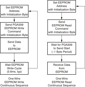
For continuous One-Wire PGA309 EEPROM writes, the controller must insert a typical 5.6ms delay between transactions, as shown in Figure 4-8. For continuous One-Wire PGA309 EEPROM reads, transactions may be repeated after the data has been received from the PGA309, as shown in Figure 4-8.
 Figure 4-8 One-Wire Access to External EEPROM
If there is an invalid communication transaction or disconnect with the EEPROM, a One-Wire EEPROM Read will be all 1s.