SLVA680A February 2015 – April 2022 ESD401 , TPD12S015 , TPD12S015A , TPD12S016 , TPD12S520 , TPD12S521 , TPD13S523 , TPD1E05U06 , TPD1E10B06 , TPD1E10B09 , TPD1S414 , TPD1S514 , TPD2E001 , TPD2E001-Q1 , TPD2E009 , TPD2E1B06 , TPD2E2U06-Q1 , TPD2EUSB30 , TPD2S017 , TPD3S014 , TPD3S044 , TPD4E001-Q1 , TPD4E004 , TPD4E02B04 , TPD4E05U06 , TPD4E05U06-Q1 , TPD4E101 , TPD4E1U06 , TPD4E6B06 , TPD4EUSB30 , TPD4F202 , TPD4S010 , TPD4S014 , TPD4S1394 , TPD4S214 , TPD5S115 , TPD5S116 , TPD6E004 , TPD6E05U06 , TPD6F002-Q1 , TPD6F003 , TPD6F202 , TPD7S019 , TPD8E003 , TPD8F003
2.4 Optimizing Ground Schemes for ESD
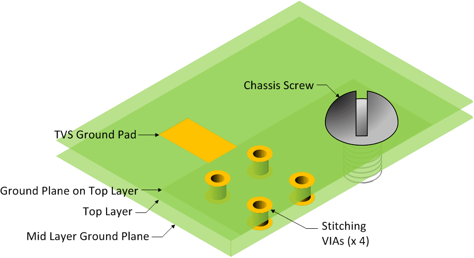
Successfully eliminating all the parasitic inductance between the ESD Source and the TVS will not be effective without a very low impedance path to ground for the TVS. The TVS ground pin should connect to a same layer ground plane that is coupled with another ground plane on an immediately adjacent layer. These ground planes should be stitched together with VIAs, with one VIA immediately adjacent to the ground pin of the TVS (see Figure 2-8).
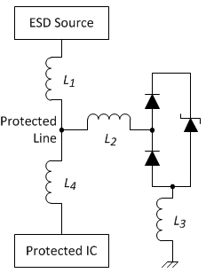
Figure 2-7 shows the PCB Inductance around a single-channel TVS (as shown earlier in Figure 2-1). This section considers only the inductance at L3. Recall that, with L2 eliminated, the voltage presented to the Protected IC during an ESD event will be VESD = Vbr_TVS + IESDRDYN(TVS) + L3(dIESD/dt) and for 8 kV, dIESD/dt = 4 × 10¹⁰. Clearly, L3 must be lowered as much as possible.
 Figure 2-7 PCB
Inductance around a Single-channel TVS
Figure 2-7 PCB
Inductance around a Single-channel TVSTo lower L3, the TVS ground pin would ideally connect directly to a coupled ground plane. Figure 2-8 shows the ground pad of a TVS connected to the top layer ground plane. There are four stitching VIAs connecting the top layer ground plane to an internal ground plane. These could connect more than one ground plane layer depending on the layer count and board design. A grounded chassis screw is located very near to the TVS ground pad as well. A grounding scheme resembling this yields a very low impedance to ground for L3.
 Figure 2-8 Two Layer
PCB - Top Ground Plane Stitched to a Mid-Layer Ground Plane
Figure 2-8 Two Layer
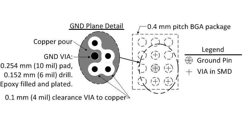
PCB - Top Ground Plane Stitched to a Mid-Layer Ground PlaneFigure 2-8 is not relevant for some types of TVSs due to package types. Those with BGA packages which have the ground pin surrounded by other pins will need to VIA to an internal ground plane, preferably to multiple, coupled ground planes. Figure 2-9 shows a TVS with such a ground pin.
 Figure 2-9 Grounding an Isolated Ground Pin in a BGA Package
VIAs need to be constructed to offer as little impedance as possible. Due to the skin effect, maximizing the surface area of the GND VIA minimizes the impedance of the path to ground. For this reason make both the VIA pad diameter and the VIA drill diameter as large as possible, thus maximizing the surface area of the outside of the VIA surface and the inside of the VIA surface. The ground plane should not be broken in the vicinity of the GND VIA. If possible, attaching the GND VIA to a ground plane on multiple layers minimizes the impedance. The GND VIA should be filled with a non-conductive filler (like epoxy) as opposed to a conductive filler, in order to keep the surface area of the inside of the VIA created by the drill. The GND VIA should be plated over at the SMD pad. Clearances between the GND VIA and non-ground planes (for example, power planes) should be kept at a minimum. This increases capacitance which lowers impedance.