SLVA680A February 2015 – April 2022 ESD401 , TPD12S015 , TPD12S015A , TPD12S016 , TPD12S520 , TPD12S521 , TPD13S523 , TPD1E05U06 , TPD1E10B06 , TPD1E10B09 , TPD1S414 , TPD1S514 , TPD2E001 , TPD2E001-Q1 , TPD2E009 , TPD2E1B06 , TPD2E2U06-Q1 , TPD2EUSB30 , TPD2S017 , TPD3S014 , TPD3S044 , TPD4E001-Q1 , TPD4E004 , TPD4E02B04 , TPD4E05U06 , TPD4E05U06-Q1 , TPD4E101 , TPD4E1U06 , TPD4E6B06 , TPD4EUSB30 , TPD4F202 , TPD4S010 , TPD4S014 , TPD4S1394 , TPD4S214 , TPD5S115 , TPD5S116 , TPD6E004 , TPD6E05U06 , TPD6F002-Q1 , TPD6F003 , TPD6F202 , TPD7S019 , TPD8E003 , TPD8F003
2.3 Routing with VIAs
It is best to route traces on the PCB from the ESD Source to the TVS without switching layers by VIA. Figure 2-5 shows two examples. In Case 1, there is no VIA between the ESD Source and the TVS, so that IESD is forced to the TVS protection pin before the VIA in the path to the Protected IC. In this case the VIA represents L4 shown in Figure 2-1. In Case 2, IESD branches between the Protected IC and the VIA to the TVS protection pin. In this case the VIA represents L2 in Figure 2-1. This practice should be avoided. The inductance of the VIA is between the TVS and the path from the ESD Source to the Protected IC. This has two detrimental effects: Since current seeks the path to ground with the least impedance, the Protected IC may take the brunt of the current in IESD and any current that does pass through the VIA will increase the voltage presented to the Protected IC by LVIA(dIESD/dt).
 Figure 2-5 Routing
with VIAs
Figure 2-5 Routing
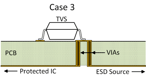
with VIAsThere may be cases where the designer has no choice but to place the TVS on a different layer than the ESD Source. Figure 2-6 shows Case 3 , a variation to Case 2. In Case 3, IESD is forced to the protection pin of the TVS before IESD has a path to the Protected IC. This is an acceptable compromise to Case 2.
 Figure 2-6 Routing
with VIAs
Figure 2-6 Routing
with VIAsThese three cases represent examples when VIAs are used between the ESD Source and the Protected IC. It is best to avoid this practice, but if necessary Case 1 is the preferred method, Case 2 should be avoided, and Case 3 is acceptable if there is no alternative.
Summary
- Avoid VIAs between the ESD Source and TVS if possible
- If a VIA is required between the ESD Source and the Protected IC, route directly from the ESD Source to the TVS before using the VIA