SNAA320B November 2019 – January 2024 LM4040-N , LM4050-N , LM4120 , LM4128 , LM4128-Q1 , LM4132 , LM4132-Q1 , REF102 , REF1925 , REF1930 , REF1933 , REF1941 , REF20-Q1 , REF200 , REF2025 , REF2030 , REF2033 , REF2041 , REF2125 , REF2912 , REF2920 , REF2925 , REF2930 , REF2933 , REF2940 , REF30 , REF3033-Q1 , REF31-Q1 , REF3112 , REF3120 , REF3125 , REF3130 , REF3133 , REF3140 , REF3212 , REF3212-EP , REF3220 , REF3220-EP , REF3225 , REF3225-EP , REF3230 , REF3230-EP , REF3233 , REF3240 , REF3312 , REF3318 , REF3320 , REF3325 , REF3330 , REF3333 , REF34-Q1 , REF3425 , REF3425-EP , REF3430 , REF3430-EP , REF3433 , REF3433-EP , REF3440 , REF3440-EP , REF3450 , REF35 , REF4132 , REF4132-Q1 , REF50 , REF5020-EP , REF5020A-Q1 , REF5025-EP , REF5025-HT , REF5025A-Q1 , REF5030A-Q1 , REF5040-EP , REF5040A-Q1 , REF5045A-Q1 , REF5050-EP , REF5050A-Q1 , REF50E , REF54 , REF6125 , REF6133 , REF6141 , REF6145 , REF6150 , REF6225 , REF6230 , REF6233 , REF6241 , REF6245 , REF6250 , REF70 , TL431LI , TL432LI , TLV431
4 DC Error Calculations
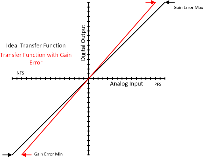
To maintain that a system meets the gain error specifications, first characterize the gain error into a usable value. This is important because gain error affects the signal chain in a different way than dynamic error and noise error. For example, when a voltage reference supplies the reference for an ADC, the DC errors of the voltage reference combines with the gain error of the ADC. When measuring a signal, this means that the gain error scales proportionally to the ADC analog signal as shown in Figure 4-1. The gain error appears as an inaccuracy on the final ADC conversion but this can be minimized with calibration. The max gain error appears closer to the positive or negative full scale value of the ADC.
 Figure 4-1 ADC Input to Output With Gain Error
An issue with characterizing the signal chain error with an integrated voltage reference is that typically internal voltage references are not fully characterized as in depth as external voltage references and often lack maximum worst case values. Due to this,calculating the worst case gain error of the system is difficult. This challenge can be resolved by using an external voltage reference. The main reason to know the extrema is because not every system has the same level of calibration. If a signal chain only has gain error calibration at 25C the gain error decreases at 25C. If the same system experiences any environmental variations then the gain error changes and is unaccounted which can take a sensitive system out of tolerance. There are many applications where the internal voltage reference is sufficient but in other applications does not exist internally.
 Figure 4-2 ADC Gain Error
There are two ways to calculate error in a system: worst-case and root sum squared (RSS). The main difference between the error calculations is how the individual errors of a system are combined. In worse case error all the errors are additive of the maximum extrema of each specification which results in an error value that encompass every device variation. The worst case error is calculated as the additive value of all the errors as shown in Equation 1 and covers all the test conditions and limits. A alternative to the worst-case method is the RSS method that is based on statistical tolerance analysis as shown in Equation 2 that applies when all the terms are uncorrelated. In the real world, the error is between the worst-case and RSS method of results but closer to the RSS result.


The total gain error for a voltage reference is a culmination of all the errors such as initial accuracy, temperature coefficient, etc. To calculate the total error, all the errors must be in common units such as ppm (parts-per million). The voltage reference total gain error can be further reduced with calibration, as calibration can eliminate the static errors such as initial accuracy and temperature drift as shown in Table 4-1. For the purposes of this example, errors such as solder shift, long term drift, load regulation, line regulation, and solder shift among others have been omitted but can be included to calculate a more accurate representation of the VREF total error. Other errors that were not mentioned can be found in Table 2-1. Table 4-1 shows how all the errors are combined using the RSS method.
| GAIN ERROR | GAIN ERROR VALUE | GAIN ERROR VALUE (ppm) |
|---|---|---|
| Initial Accuracy | 0.05% | 500 |
| Temperature Drift (TempCo) | 6ppm/°C | 990 (40°C to 125°C) |
| Temperature Drift Post Calibration (80% Reduction) | 1.2ppm/°C | 198 (40°C to 125°C) |
| Thermal Hysteresis (TempHyst) | Cycle 1: 30ppm, Cycle 2: 10ppm | 40 |
| 1/f noise | 15uVP-P | 15 |
| Worst Case Total | 0.1545% | 1545 |
| RSS Total | 0.111% | 1110 |
| RSS Total with 25C Calibration | 0.0991% | 991 |
| RSS Total with 25C and TempCo Calibration | 0.0202% | 202 |
In Table 4-1 You can see the comparison of total gain error under different conditions and the importance of calibration. By using Equation 3 and a known ADC resolution, the LSBs that is affected by the gain error of the signal chain can be calculated.
