SPRUIQ4 May 2019 TMS320F280021 , TMS320F280021-Q1 , TMS320F280023 , TMS320F280023-Q1 , TMS320F280023C , TMS320F280025 , TMS320F280025-Q1 , TMS320F280025C , TMS320F280025C-Q1 , TMS320F280040-Q1 , TMS320F280040C-Q1 , TMS320F280041 , TMS320F280041-Q1 , TMS320F280041C , TMS320F280041C-Q1 , TMS320F280045 , TMS320F280048-Q1 , TMS320F280048C-Q1 , TMS320F280049 , TMS320F280049-Q1 , TMS320F280049C , TMS320F280049C-Q1 , TMS320F28374D , TMS320F28374S , TMS320F28375D , TMS320F28375S , TMS320F28375S-Q1 , TMS320F28376D , TMS320F28376S , TMS320F28377D , TMS320F28377D-EP , TMS320F28377D-Q1 , TMS320F28377S , TMS320F28377S-Q1 , TMS320F28378D , TMS320F28378S , TMS320F28379D , TMS320F28379D-Q1 , TMS320F28379S
- Introduction
- 1Getting Familiar With the Kit
-
2Hardware Overview
- 2.1 IDDK Evaluation Board
- 2.2 Functional Blocks
- 2.3 Processor Section
- 2.4 Control Processor Slot – H1
- 2.5 Expansion Processor Slots
- 2.6 Position Encoder Suite
- 2.7 Current Sensor Suite
- 2.8 Power Supplies and GND Plane Configurations
- 2.9 Rectifier and Inverter
- 2.10 DACs
- 2.11 Power Stage Disable Circuits
- 3Hardware Resource Mapping
2.1 IDDK Evaluation Board
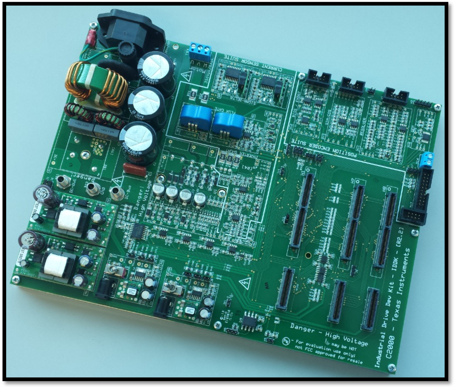
Figure 2-1 shows that the IDDK evaluation board is an open board without enclosures.
 Figure 2-1 IDDK EVM Kit
 The board can be divided into the following functional blocks:
- The processor (CPU) block for control, real-time connectivity, and functional safety
- The position encoder suite
- The current sensor suite
- The power inverter and rectifier
- Onboard power supplies
For experimentation, three GND planes are on the board: one plane is for safety and connectivity circuits, another plane is for control and interface, and a third plane is for high power circuits. Provisions are on the board to connect GND planes. If the control GND is tied to the power GND, ensure that position sensors and encoders connected to the board are properly grounded to earth.
NOTE
IDDK offers reconfigurable GND planes, an interprocessor interface, and power stage control. The GND plane configurations can change depending on the style of current sensing and position sensing in the drive solution. The default configuration of the GND planes is only intended for users to develop MCU software drivers to evaluate their topologies. TI does not recommend this configuration for any final drive design or solution. You can select and develop control strategies based on the GND plane reconfigurations and interprocessor interface.
The default isolation/GND configuration of revision R2.2.1 of this evaluation board is set up to have all controlCARDs (H1, H7, and H8) and their interface circuits be separate from the high voltage inverter GND. controlCARDS H1, H7, and H8 have COLD GND, while the inverter has HOT GND.
In the previous release of the board, IDDK R2.2, the control GND was tied to HOT GND in R2.2. In R2.2.1, control GND is tied to COLD GND. Take care while switching between these two boards considering the changes in control GND configuration..