SPRUIS4E March 2022 – January 2024
- 1
- Jacinto7 J721E/DRA829/TDA4VM Evaluation Module (EVM)
- Trademarks
- 1Introduction
- 2J721E EVM Overview
- 3EVM User Setup/Configuration
-
4J721E EVM Hardware Architecture
- 4.1 J721E EVM Hardware Top level Diagram
- 4.2 J721E EVM Interface Mapping
- 4.3 I2C Address Mapping
- 4.4 GPIO Mapping
- 4.5 Power Supply
- 4.6 Reset
- 4.7 Clock
- 4.8 Memory Interfaces
- 4.9 MCU Ethernet Interface
- 4.10 QSGMII Ethernet Interface
- 4.11 PCIe Interface
- 4.12 USB Interface
- 4.13 CAN Interface
- 4.14 FPD Interface (Audio Deserializer)
- 4.15 FPD Panel Interface (DSI Video Serializer)
- 4.16 Display Serial Interface (DSI) FPC
- 4.17 Audio Interface
- 4.18 Display Port Interface
- 4.19 MLB Interface
- 4.20 I3C Interface
- 4.21 ADC Interface
- 4.22 RTC Interface
- 4.23 Apple Authentication Header
- 4.24 EVM Expansion Connectors
- 4.25 ENET Expansion Connector
- 4.26 CSI Expansion Connector
- 5Revision History
4.19 MLB Interface
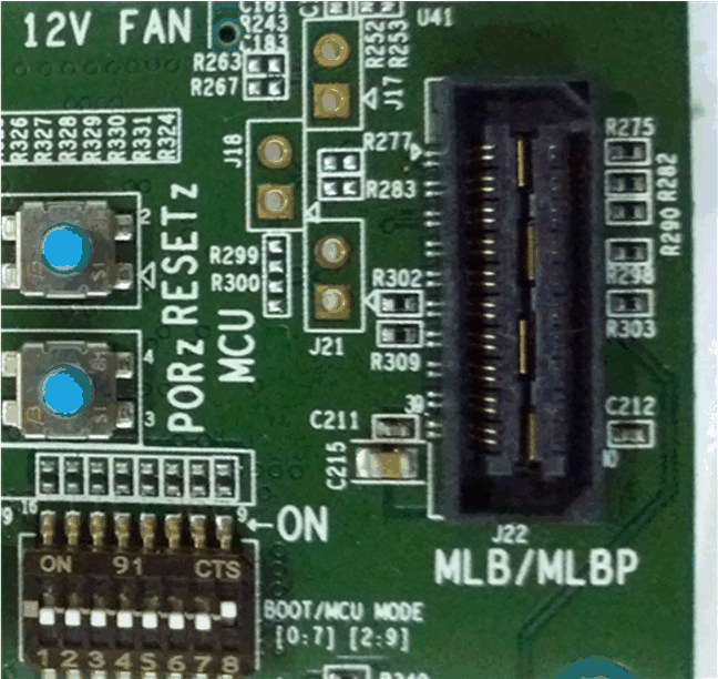
Common Processor board supports for Media Local Bus (MLB) interface.
Differential pairs of MLB signals from J721E SoC are routed to Samtec header Mfr. Part# QSH-020-01-L-D-DP-A-K. This interfaces is designed to mate with MicroChip’s MLB Physical interface board. The differential signals are routed with a characteristic impedance of 100E and also a Pull up and Pull-down option is provided for the N and P signals respectively. The reset signal that comes from the expander (I2C ADD# 0x22, I2C0) is availed with a pull down to avoid floating, and the interrupt signal is equipped with a pull up and routed to J721E SoM.
The 12 V and 3.3 V are drawn from the CP board to the connector; the I2C control is provided to the MLB Header from I2C0 port of J721E SoC.
 Figure 4-39 MLB Interface
Connector
Figure 4-39 MLB Interface
ConnectorTable 4-23 lists the pinout for MLB Header J22 (QSH-020-01-L-D-DP-A).
| Pin No | Signal | Pin No | Signal |
|---|---|---|---|
| 1 | MLB0_MLBSIG_N | 2 | H_MLB0_MLBCLK |
| 3 | MLB0_MLBSIG_P | 4 | NC |
| 5 | NC | 6 | H_MLB0_MLBSIG |
| 7 | NC | 8 | NC |
| 9 | MLB0_MLBDAT_N | 10 | H_MLB0_MLBDAT |
| 11 | MLB0_MLBDAT_P | 12 | NC |
| 13 | NC | 14 | NC |
| 15 | NC | 16 | H_MLB0_REFCLK |
| 17 | MLB0_MLBCLK_N | 18 | NC |
| 19 | MLB0_MLBCLK_P | 20 | NC |
| 21 | DGND | 22 | DGND |
| 23 | NC | 24 | MLB0_GPIO0 |
| 25 | MLB_RSTz | 26 | NC |
| 27 | NC | 28 | NC |
| 29 | NC | 30 | NC |
| 31 | NC | 32 | NC |
| 33 | I2C0_SCL | 34 | MLB_INT# |
| 35 | I2C0_SDA | 36 | NC |
| 37 | VSYS_IO_3V3 | 38 | VSYS_IO_3V3 |
| 39 | VSYS_IO_3V3 | 40 | VCC_12V0 |