SPRUIS4E March 2022 – January 2024
- 1
- Jacinto7 J721E/DRA829/TDA4VM Evaluation Module (EVM)
- Trademarks
- 1Introduction
- 2J721E EVM Overview
- 3EVM User Setup/Configuration
-
4J721E EVM Hardware Architecture
- 4.1 J721E EVM Hardware Top level Diagram
- 4.2 J721E EVM Interface Mapping
- 4.3 I2C Address Mapping
- 4.4 GPIO Mapping
- 4.5 Power Supply
- 4.6 Reset
- 4.7 Clock
- 4.8 Memory Interfaces
- 4.9 MCU Ethernet Interface
- 4.10 QSGMII Ethernet Interface
- 4.11 PCIe Interface
- 4.12 USB Interface
- 4.13 CAN Interface
- 4.14 FPD Interface (Audio Deserializer)
- 4.15 FPD Panel Interface (DSI Video Serializer)
- 4.16 Display Serial Interface (DSI) FPC
- 4.17 Audio Interface
- 4.18 Display Port Interface
- 4.19 MLB Interface
- 4.20 I3C Interface
- 4.21 ADC Interface
- 4.22 RTC Interface
- 4.23 Apple Authentication Header
- 4.24 EVM Expansion Connectors
- 4.25 ENET Expansion Connector
- 4.26 CSI Expansion Connector
- 5Revision History
4.13 CAN Interface
The four CAN ports of J721E SoC (MCU_MCAN0, MCU_MCAN1, MCAN0, and MCAN2) is supported on the Common Processor board as explained below.
MCU CAN0
The MCU CAN0 port of J721E SoC is connected to the CAN transceiver with Wake function supported device TCAN1043-Q1. A 2-pin header J29 (68002-202HLF) is provided inline for user probe option.
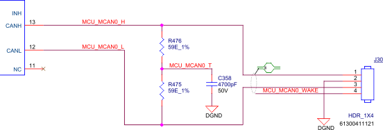
The output of the CAN transceiver is terminated to a 4-pin header J30 (61300411121).
The signals MCU_MCAN0_H and MCU_MCAN0_L are routed as differential signals with 120E impedance with split termination. This Split termination improves the electromagnetic emissions behavior of the network by eliminating fluctuations in the bus common-mode voltages at the start and end of message transmissions.
 Figure 4-31 MCU CAN0 Interface
VSYS_MCU_5V0 to the CAN transceiver is generated using a Step-Up converter TPS61240DRV by giving VSYS_3V3 as input supply to the converter.
The STB signal is an active low signal held low with integrated pull down by default.
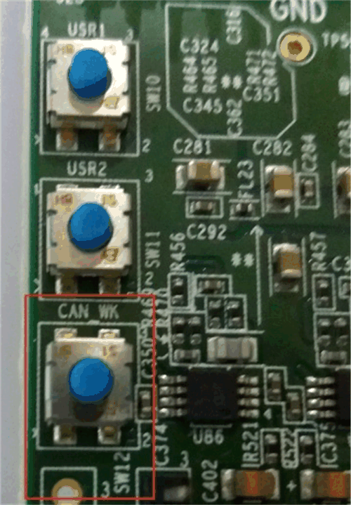
Hardware WAKEn input for the CAN interface is provided using a push-button SW12 available on the Common processor board bottom left corner. However, the MCU_CAN0 wake feature is disabled by default (resistor population). Only CAN wake-up supported is from MAIN domain.
MCU CAN1
The MCU CAN1 port of J721E SoC is connected to the CAN transceiver Mfr. Part# TCAN1042HGVD. A 2-pin header J34 (68002-202HLF) is provided inline for user probe option. This port does not support WAKE function. The signals MCU_MCAN1_H and MCU_MCAN1_L are terminated to a 3-pin header J31 (FCI: 68001-403HLF) with 120E split termination.
The STB signal is an active High signal held high with external pull up by default. The GPIO control from MCU domain provided to pull the line low.
MAIN CAN0 (Supports WAKE function)
The MAIN CAN0 port of J721E SoC is connected to the CAN transceiver with Wake function supported device TCAN1043-Q1. A 2-pin header J24 (68002-202HLF) is provided inline for user probe option.
The output of the CAN transceiver is terminated to a 4-pin header J27 (61300411121).
The signals MCAN0_H and MCAN0_L are routed as differential signals with 120E impedance with split termination. The STB signal is an active low signal held low with integrated pull down by default.
The VCC supply (5V) to the transceiver is derived from a Step-Up converter.
Hardware WAKEn input for the CAN interface is provided using a push-button SW12.
 Figure 4-32 CAN Wake Push Button
The CAN Wake signals of both MCU CAN0 and MAIN CAN0 transceivers are tied together and limited the voltage level to 1.8V using a Zener diode and terminated to SOM -CP B2B connector.
MAIN CAN2
The MAIN CAN2 port of J721E SoC is connected to the CAN transceiver Mfr. Part# TCAN1042HGVD. A 2-pin header J25 (68002-202HLF) is provided inline for user probe option. This port does not support WAKE function. The signals MCAN2_H and MCAN2_L are terminated to a 3-pin header J28 (68001-403HLF) with 120E split termination.
The STB signal is an active High signal held high with external pull up by default. The GPIO control from MAIN domain provided to pull the line low.
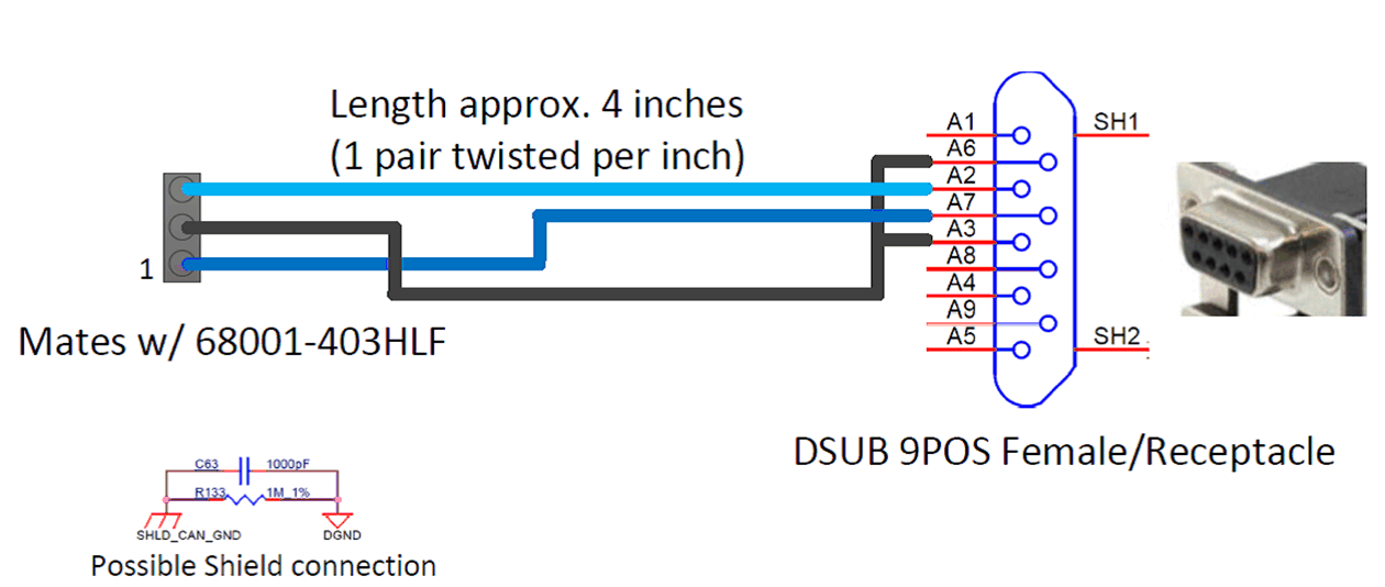
To interface these CAN signals to Test system, the below given custom converter to be prepared.
 Figure 4-33 CAN Header Connections to DB9/Test Instrument