SPRUIS4E March   2022  – January 2024


  1.   1
  2.   Jacinto7 J721E/DRA829/TDA4VM Evaluation Module (EVM)
  3.   Trademarks
  4. 1Introduction
    1. 1.1 Key Features
    2. 1.2 Thermal Compliance
    3. 1.3 REACH Compliance
    4. 1.4 EMC, EMI, and ESD Compliance
  5. 2J721E EVM Overview
    1. 2.1 J721E EVM Board Identification
    2. 2.2 J721E SOM Component Identification
    3. 2.3 Jacinto7 Common Processor Components Identification
    4. 2.4 Quad Ethernet Components Identification
  6. 3EVM User Setup/Configuration
    1. 3.1 Power Requirements
    2. 3.2 Power ON Switch and Power LEDs
      1. 3.2.1 Over Voltage and Under Voltage Protection Circuit
      2. 3.2.2 Power Regulators and Power Status LEDs
    3. 3.3 EVM Reset/Interrupt Push Buttons
    4. 3.4 EVM DIP Switches
      1. 3.4.1 EVM Configuration DIP Switch
      2. 3.4.2 SOM Configuration DIP Switch
      3. 3.4.3 Boot Modes
      4. 3.4.4 Other Selection Switches
    5. 3.5 EVM UART/COM Port Mapping
    6. 3.6 JTAG Emulation
  7. 4J721E EVM Hardware Architecture
    1. 4.1  J721E EVM Hardware Top level Diagram
    2. 4.2  J721E EVM Interface Mapping
    3. 4.3  I2C Address Mapping
    4. 4.4  GPIO Mapping
    5. 4.5  Power Supply
      1. 4.5.1 Power Sequencing
      2. 4.5.2 Voltage Supervisor
      3. 4.5.3 DDR I/O Voltage Selection
        1. 4.5.3.1 J721E SoC S2R Logic Flow Diagram
        2. 4.5.3.2 J721E SoC MCU Only Operation
        3. 4.5.3.3 Power Monitoring
    6. 4.6  Reset
    7. 4.7  Clock
      1. 4.7.1 Processor’s Primary Clock
      2. 4.7.2 Processor’s Secondary/SERDES Ref Clock
      3. 4.7.3 EVM Peripheral Ref Clock
    8. 4.8  Memory Interfaces
      1. 4.8.1 LPDDR4 Interface
      2. 4.8.2 OSPI Interface
      3. 4.8.3 UFS Interface
      4. 4.8.4 MMC Interface
        1. 4.8.4.1 MMC0 - eMMC Interface
        2. 4.8.4.2 MMC1 – Micro SD Interface
      5. 4.8.5 Board ID EEPROM Interface
      6. 4.8.6 Boot EEPROM Interface
    9. 4.9  MCU Ethernet Interface
      1. 4.9.1 Gigabit Ethernet PHY Default Configuration
    10. 4.10 QSGMII Ethernet Interface
    11. 4.11 PCIe Interface
      1. 4.11.1 X1 Lane PCIe Interface
      2. 4.11.2 X2 Lane PCIe Interface
      3. 4.11.3 M.2 PCIe Interface
    12. 4.12 USB Interface
      1. 4.12.1 USB 3.1 Interface
      2. 4.12.2 USB 2.0 Interface
      3. 4.12.3 USB 3.0 Micro AB Interface (Reserved Port)
    13. 4.13 CAN Interface
    14. 4.14 FPD Interface (Audio Deserializer)
    15. 4.15 FPD Panel Interface (DSI Video Serializer)
    16. 4.16 Display Serial Interface (DSI) FPC
    17. 4.17 Audio Interface
    18. 4.18 Display Port Interface
    19. 4.19 MLB Interface
    20. 4.20 I3C Interface
    21. 4.21 ADC Interface
    22. 4.22 RTC Interface
    23. 4.23 Apple Authentication Header
    24. 4.24 EVM Expansion Connectors
    25. 4.25 ENET Expansion Connector
      1. 4.25.1 Power Requirements
      2. 4.25.2 Clock
        1. 4.25.2.1 Main Clock
        2. 4.25.2.2 Optional Clock
      3. 4.25.3 Reset Signals
      4. 4.25.4 Ethernet Interface
        1. 4.25.4.1 Quad Port SGMII PHY Default Configuration
      5. 4.25.5 Board ID EEPROM Interface
    26. 4.26 CSI Expansion Connector
  8. 5Revision History

OSPI Interface

The J721E SOM has 512 Mbit OSPI memory device of part number MT35XU512ABA1G12-0SIT connected to OSPI0 interface of J721E processor. The OSPI interface supports single and double data rates with memory speed up to 166 MHz SDR and 200 MHz DDR.

The SOM board also supports an option to include Hyper Flash + Hyper RAM Mfr. Part# S71KS512SC0, which is a 512 Mb flash + 64 Mb DRAM. 12-bit Active mux TS3DDR3812RUAR is provided to select either OSPI or HBMC interface. The selection of OSPI and hyper flash will be done by using a DIP (SW3) switch that is populated on the CP board. For more information, see Section 3.4.1.
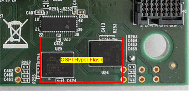
GUID-F9684B35-0F8F-40DF-8ED1-21468AFEFCAD-low.gifFigure 4-11 J721E SoM OSPI and Hyper Flash