SPRUIS4E March   2022  – January 2024


  1.   1
  2.   Jacinto7 J721E/DRA829/TDA4VM Evaluation Module (EVM)
  3.   Trademarks
  4. 1Introduction
    1. 1.1 Key Features
    2. 1.2 Thermal Compliance
    3. 1.3 REACH Compliance
    4. 1.4 EMC, EMI, and ESD Compliance
  5. 2J721E EVM Overview
    1. 2.1 J721E EVM Board Identification
    2. 2.2 J721E SOM Component Identification
    3. 2.3 Jacinto7 Common Processor Components Identification
    4. 2.4 Quad Ethernet Components Identification
  6. 3EVM User Setup/Configuration
    1. 3.1 Power Requirements
    2. 3.2 Power ON Switch and Power LEDs
      1. 3.2.1 Over Voltage and Under Voltage Protection Circuit
      2. 3.2.2 Power Regulators and Power Status LEDs
    3. 3.3 EVM Reset/Interrupt Push Buttons
    4. 3.4 EVM DIP Switches
      1. 3.4.1 EVM Configuration DIP Switch
      2. 3.4.2 SOM Configuration DIP Switch
      3. 3.4.3 Boot Modes
      4. 3.4.4 Other Selection Switches
    5. 3.5 EVM UART/COM Port Mapping
    6. 3.6 JTAG Emulation
  7. 4J721E EVM Hardware Architecture
    1. 4.1  J721E EVM Hardware Top level Diagram
    2. 4.2  J721E EVM Interface Mapping
    3. 4.3  I2C Address Mapping
    4. 4.4  GPIO Mapping
    5. 4.5  Power Supply
      1. 4.5.1 Power Sequencing
      2. 4.5.2 Voltage Supervisor
      3. 4.5.3 DDR I/O Voltage Selection
        1. 4.5.3.1 J721E SoC S2R Logic Flow Diagram
        2. 4.5.3.2 J721E SoC MCU Only Operation
        3. 4.5.3.3 Power Monitoring
    6. 4.6  Reset
    7. 4.7  Clock
      1. 4.7.1 Processor’s Primary Clock
      2. 4.7.2 Processor’s Secondary/SERDES Ref Clock
      3. 4.7.3 EVM Peripheral Ref Clock
    8. 4.8  Memory Interfaces
      1. 4.8.1 LPDDR4 Interface
      2. 4.8.2 OSPI Interface
      3. 4.8.3 UFS Interface
      4. 4.8.4 MMC Interface
        1. 4.8.4.1 MMC0 - eMMC Interface
        2. 4.8.4.2 MMC1 – Micro SD Interface
      5. 4.8.5 Board ID EEPROM Interface
      6. 4.8.6 Boot EEPROM Interface
    9. 4.9  MCU Ethernet Interface
      1. 4.9.1 Gigabit Ethernet PHY Default Configuration
    10. 4.10 QSGMII Ethernet Interface
    11. 4.11 PCIe Interface
      1. 4.11.1 X1 Lane PCIe Interface
      2. 4.11.2 X2 Lane PCIe Interface
      3. 4.11.3 M.2 PCIe Interface
    12. 4.12 USB Interface
      1. 4.12.1 USB 3.1 Interface
      2. 4.12.2 USB 2.0 Interface
      3. 4.12.3 USB 3.0 Micro AB Interface (Reserved Port)
    13. 4.13 CAN Interface
    14. 4.14 FPD Interface (Audio Deserializer)
    15. 4.15 FPD Panel Interface (DSI Video Serializer)
    16. 4.16 Display Serial Interface (DSI) FPC
    17. 4.17 Audio Interface
    18. 4.18 Display Port Interface
    19. 4.19 MLB Interface
    20. 4.20 I3C Interface
    21. 4.21 ADC Interface
    22. 4.22 RTC Interface
    23. 4.23 Apple Authentication Header
    24. 4.24 EVM Expansion Connectors
    25. 4.25 ENET Expansion Connector
      1. 4.25.1 Power Requirements
      2. 4.25.2 Clock
        1. 4.25.2.1 Main Clock
        2. 4.25.2.2 Optional Clock
      3. 4.25.3 Reset Signals
      4. 4.25.4 Ethernet Interface
        1. 4.25.4.1 Quad Port SGMII PHY Default Configuration
      5. 4.25.5 Board ID EEPROM Interface
    26. 4.26 CSI Expansion Connector
  8. 5Revision History

USB 3.1 Interface

USB Super speed signals from SERDES3 port of J7E21E SoC are connected to USB Type C connector (2012670005). A CC and PD controller Mfr. Part# TUSB321RWBR and PTPS25830QWRHBTQ1 are used for CC detect and power delivery. This CC controller supports Dual Role Port (DRP), Downstream Facing Port (DFP) and Upstream Facing Port (UFP) modes, In CP board DRP, DFP and UFP modes can be selected through an EVM Configuration dip switch (SW3). The Dip switch settings are given in Table 3-5Table 6.
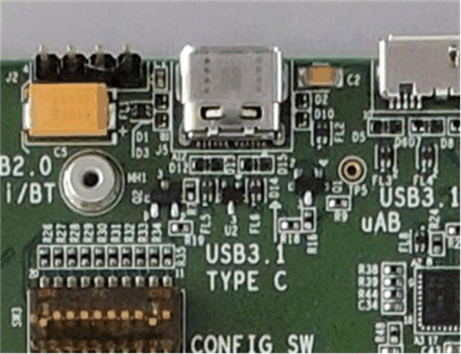
GUID-AD8E8CEB-929A-41E0-9386-47221876DA90-low.gifFigure 4-26 USB3.1 Type C Interface

The AC coupling capacitors are provided on TX lines of Super speed signals, and common mode filters (MCZ1210DH900L2TA0G) are used at all the differential pairs. ESD protection diodes are provided on all required USB Signals (TPD1E05U06DPY for super speed signals and TPD2E2U06-Q1 for CC pins). TUSB321‘s Current Mode pin is pulled high through 499K resistor to set the Maximum Current Iout to 1.5A.
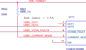
GUID-DF44FDD6-CBC2-431A-AD55-D9258609DFE6-low.gifFigure 4-27 Type C Power Delivery Current Settings

The control signals for Powerdown and VBUS enable are given from I2C GPIO Expander2 (I2C add: 0x22 - P03) and the SoC DRVVBUS, respectively.