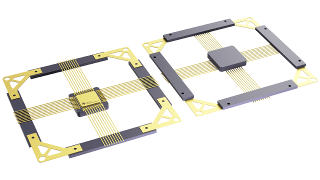
36-pin (HFG) package image

5962-1620701VXC ACTIVE

1:10 high speed clock buffer with selectable input clock driver

ACTIVE barcode LOT/DATE Lot and date code selection may be available

Pricing

Qty Price
+

Quality information

Rating Space
RoHS Yes
REACH Yes
MSL rating / Peak reflow Level-NC-NC-NC
Quality, reliability
& packaging information

Information included:

  • RoHS
  • REACH
  • Device marking
  • Lead finish / Ball material
  • MSL rating / Peak reflow
  • MTBF/FIT estimates
  • Material content
  • Qualification summary
  • Ongoing reliability monitoring
View or download
Additional manufacturing information

Information included:

  • Fab location
  • Assembly location
View

Export classification

*For reference only

  • US ECCN: EAR99

Packaging information

Package | Pins CFP (HFG) | 36
Operating temperature range (°C) -55 to 125
Package qty | Carrier 10 | JEDEC TRAY (5+1)

Features for the CDCLVP111-SP

  • Distributes One Differential Clock Input Pair LVPECL to 10 Differential LVPECL
  • Fully Compatible With LVECL and LVPECL
  • Supports a Wide Supply Voltage Range From 2.375 V to 3.8 V
  • Selectable Clock Input Through CLK_SEL
  • Low-Output Skew (Typical 15 ps) for Clock-Distribution Applications
    • Additive Jitter Less Than 1 ps
    • Propagation Delay Less Than 355 ps
    • Open Input Default State
    • LVDS, CML, SSTL input Compatible
  • VBB Reference Voltage Output for Single-Ended Clocking
  • Frequency Range From DC to 3.5 GHz
  • Supports Defense, Aerospace, and Medical Applications
    • Controlled Baseline
    • One Assembly and Test Site
    • One Fabrication Site
    • Available in Military (–55°C to 125°C) Temperature Range(1)
    • Extended Product Life Cycle
    • Extended Product-Change Notification
    • Product Traceability

Description for the CDCLVP111-SP

The CDCLVP111-SP clock driver distributes one differential clock pair of LVPECL input, (CLK0, CLK1) to ten pairs of differential LVPECL clock (Q0, Q9) outputs with minimum skew for clock distribution. The CDCLVP111-SP can accept two clock sources into an input multiplexer. The CDCLVP111-SP is specifically designed for driving 50-Ω transmission lines. When an output pin is not used, leaving it open is recommended to reduce power consumption. If only one of the output pins from a differential pair is used, the other output pin must be identically terminated to 50 Ω.

The VBB reference voltage output is used if single-ended input operation is required. In this case, the VBB pin should be connected to CLK0 and bypassed to GND via a 10-nF capacitor.

For high-speed performance, the differential mode is strongly recommended.

The CDCLVP111-SP is characterized for operation from –55°C to 125°C.
Pricing

Qty Price
+

Carrier options

You can choose different carrier options based on the quantity of parts, including full reel, custom reel, cut tape, tube or tray.

A custom reel is a continuous length of cut tape from one reel to maintain lot- and date-code traceability, built to the exact quantity requested. Following industry standards, a brass shim connects an 18-inch leader and trailer on both sides of the cut tape for direct feeding into automated assembly machines. TI includes a reeling fee for custom reel orders.

Cut tape is a length of tape cut from a reel. TI may fulfill orders using multiple strips of cut tapes or boxes to satisfy the quantity requested.

TI often ships tube or tray devices inside a box or in the tube or tray, depending on inventory availability. We pack all tapes, tubes or sample boxes according to internal electrostatic discharge and moisture-sensitivity-level protection requirements.

Learn more

Lot and date code selection may be available

Add a quantity to your cart and begin the checkout process to view the options available to select lot or date codes from existing inventory.

Learn more