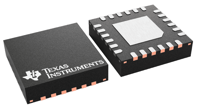
Packaging information
| Package | Pins VQFN (RGE) | 24 |
| Operating temperature range (°C) -40 to 85 |
| Package qty | Carrier 3,000 | LARGE T&R |
Features for the CDCP1803
- Distributes One Differential Clock Input to Three LVPECL Differential Clock Outputs
- Programmable Output Divider for Two LVPECL Outputs
- Low-Output Skew 15 ps (Typical)
- VCC Range 3 V–3.6 V
- Signaling Rate Up to 800-MHz LVPECL
- Differential Input Stage for Wide Common-Mode Range
- Provides VBB Bias Voltage Output for Single-Ended Input Signals
- Receiver Input Threshold ±75 mV
- 24-Terminal QFN Package (4 mm × 4 mm)
- Accepts Any Differential Signaling:
LVDS, HSTL, CML, VML, SSTL-2, and
Single-Ended: LVTTL/LVCMOS
Description for the CDCP1803
The CDCP1803 clock driver distributes one pair of differential clock inputs to three pairs of LVPECL differential clock outputs Y[2:0] and Y[2:0] with minimum skew for clock distribution. The CDCP1803 is specifically designed for driving 50-Ω transmission lines.
The CDCP1803 has three control terminals, S0, S1, and S2, to select different output mode settings; see for details. The CDCP1803 is characterized for operation from –40°C to 85°C. For use in single-ended driver applications, the CDCP1803 also provides a VBB output terminal that can be directly connected to the unused input as a common-mode voltage reference.