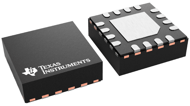
Packaging information
| Package | Pins VQFN (RGT) | 16 |
| Operating temperature range (°C) -40 to 125 |
| Package qty | Carrier 250 | SMALL T&R |
Features for the LMK00804B-Q1
- AEC-Q100 qualified with the following results:
- Device temperature grade 1: –40°C to +125°C, TA
- Four LVCMOS/LVTTL outputs supporting 1.5-V to 3.3-V
levels
- Additive jitter: 0.1-ps RMS (typical) at 40 MHz
- Noise floor: –168 dBc/Hz (typical) at 40 MHz
- Output frequency: 350 MHz (maximum)
- Output skew: 35 ps (maximum)
- Part-to-part skew: 550 ps (maximum)
- Two selectable
inputs
- CLK_P, CLK_N pair accepts LVPECL, LVDS, HCSL, SSTL, LVHSTL, or LVCMOS/LVTTL
- LVCMOS_CLK accepts LVCMOS/LVTTL
- Synchronous clock enable
- Core/output power supplies:
- 3.3 V/3.3 V
- 3.3 V/2.5 V
- 3.3 V/1.8 V
- 3.3 V/1.5 V
- Package: 16-pin VQFN
Description for the LMK00804B-Q1
The LMK00804B-Q1 is a high-performance clock fan-out buffer and level translator that can distribute up to four LVCMOS/LVTTL outputs (3.3-V, 2.5-V, 1.8-V, or 1.5-V levels) from one of two selectable inputs that can accept differential or single-ended inputs. The clock enable input is synchronized internally to eliminate runt or glitch pulses on the outputs when the clock enable terminal is asserted or deasserted. The outputs are held in logic low state when the clock is disabled. The LMK00804B-Q1 can also distribute a low-jitter clock across four transceivers and can improve the overall target detection and resolution in a cascaded mmWave radar system.