SGLS307P July 2006 – February 2018 TLK2711-SP
PRODUCTION DATA.
- 1 Features
- 2 Applications
- 3 Description
- 4 Revision History
- 5 Description (continued)
- 6 Pin Configuration and Functions
-
7 Specifications
- 7.1 Absolute Maximum Ratings
- 7.2 ESD Ratings
- 7.3 Recommended Operating Conditions
- 7.4 Thermal Information
- 7.5 TTL Input Electrical Characteristics
- 7.6 Transmitter/Receiver Electrical Characteristics
- 7.7 Reference Clock (TXCLK) Timing Requirements
- 7.8 TTL Output Switching Characteristics
- 7.9 Typical Characteristics
-
8 Detailed Description
- 8.1 Overview
- 8.2 Functional Block Diagram
- 8.3
Feature Description
- 8.3.1 Transmit Interface
- 8.3.2 Transmit Data Bus
- 8.3.3 Data Transmission Latency
- 8.3.4 8-Bit/10-Bit Encoder
- 8.3.5 Pseudo-Random Bit Stream (PRBS) Generator
- 8.3.6 Parallel to Serial
- 8.3.7 High-Speed Data Output
- 8.3.8 Receive Interface
- 8.3.9 Receive Data Bus
- 8.3.10 Data Reception Latency
- 8.3.11 Serial to Parallel
- 8.3.12 Comma Detect and 8-Bit/10-Bit Decoding
- 8.3.13 LOS Detection
- 8.3.14 PRBS Verification
- 8.3.15 Reference Clock Input
- 8.3.16 Operating Frequency Range
- 8.3.17 Testability
- 8.3.18 Loopback Testing
- 8.3.19 BIST
- 8.3.20 Power-On Reset
- 8.4 Device Functional Modes
- 9 Application and Implementation
- 10Power Supply Recommendations
- 11Layout
- 12Device and Documentation Support
- 13Mechanical, Packaging, and Orderable Information
Package Options
Mechanical Data (Package|Pins)
- HFG|68
Thermal pad, mechanical data (Package|Pins)
Orderable Information
8.3.7 High-Speed Data Output
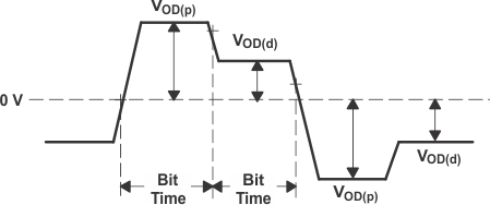
The high-speed data output driver consists of a voltage mode logic (VML) differential pair optimized for a 50-Ω impedance environment. The magnitude of the differential-pair signal swing is compatible with pseudo emitter coupled logic (PECL) levels when AC coupled. The line can be directly coupled or AC coupled. See Figure 13 and Figure 14 for termination details. The outputs also provide preemphasis to compensate for AC loss when driving a cable or PCB backplane trace over a long distance (see Figure 9). The level of preemphasis is controlled by PRE (see Table 2).
 Figure 9. Output Voltage Under Preemphasis (VTXP to VTXN)
Table 2. Programmable Preemphasis
| PRE | PREEMPHASIS LEVEL (%) VOD(P), VOD(D)(1) |
|---|---|
| 0 | 5% |
| 1 | 20% |
(1) VOD(p): Voltage swing when there is a transition in the data stream.
VOD(d): Voltage swing when there is no transition in the data stream.
VOD(d): Voltage swing when there is no transition in the data stream.