SWRS201C January 2017 – March 2025 CC2640R2F-Q1
PRODUCTION DATA
- 1
- 1 Features
- 2 Applications
- 3 Description
- 4 Functional Block Diagram
- 5 Device Comparison
- 6 Pin Configuration and Functions
-
7 Specifications
- 7.1 Absolute Maximum Ratings
- 7.2 ESD Ratings
- 7.3 Recommended Operating Conditions
- 7.4 Power Consumption Summary
- 7.5 General Characteristics
- 7.6 1Mbps GFSK (Bluetooth Low Energy Technology)—RX
- 7.7 1Mbps GFSK (Bluetooth Low Energy Technology)—TX
- 7.8 24MHz Crystal Oscillator (XOSC_HF)
- 7.9 32.768kHz Crystal Oscillator (XOSC_LF)
- 7.10 48MHz RC Oscillator (RCOSC_HF)
- 7.11 32kHz RC Oscillator (RCOSC_LF)
- 7.12 ADC Characteristics
- 7.13 Temperature Sensor
- 7.14 Battery Monitor
- 7.15 Continuous Time Comparator
- 7.16 Low-Power Clocked Comparator
- 7.17 Programmable Current Source
- 7.18 Synchronous Serial Interface (SSI)
- 7.19 DC Characteristics
- 7.20 Thermal Resistance Characteristics for RGZ Package
- 7.21 Timing Requirements
- 7.22 Switching Characteristics
- 7.23 Typical Characteristics
- 8 Detailed Description
- 9 Application, Implementation, and Layout
- 10Device and Documentation Support
- 11Revision History
- 12Mechanical, Packaging, and Orderable Information
Package Options
Refer to the PDF data sheet for device specific package drawings
Mechanical Data (Package|Pins)
- RGZ|48
Thermal pad, mechanical data (Package|Pins)
Orderable Information
7.18 Synchronous Serial Interface (SSI)
Tc = 25°C, VDDS = 3.0V, unless otherwise noted.
| PARAMETER | TEST CONDITIONS | MIN | TYP | MAX | UNIT |
|---|---|---|---|---|---|
| S1(1) tclk_per (SSIClk period) | Device operating as SLAVE | 12 | 65024 | system clocks | |
| S2(1) tclk_high (SSIClk high time) | Device operating as SLAVE | 0.5 | tclk_per | ||
| S3(1) tclk_low (SSIClk low time) | Device operating as SLAVE | 0.5 | tclk_per | ||
| S1 (TX only)(1) tclk_per (SSIClk period) | One-way communication to SLAVE: Device operating as MASTER | 4 | 65024 | system clocks | |
| S1 (TX and RX)(1) tclk_per (SSIClk period) | Normal duplex operation: Device operating as MASTER | 8 | 65024 | system clocks | |
| S2(1) tclk_high (SSIClk high time) | Device operating as MASTER | 0.5 | tclk_per | ||
| S3(1) tclk_low(SSIClk low time) | Device operating as MASTER | 0.5 | tclk_per |
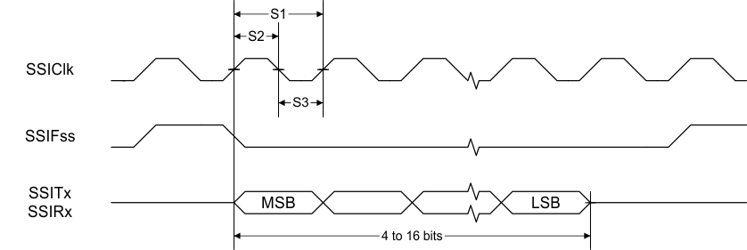
 Figure 7-1 SSI Timing for TI Frame Format (FRF = 01), Single Transfer Timing Measurement
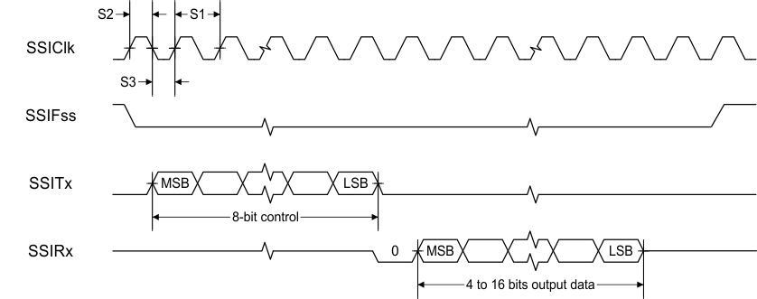
 Figure 7-2 SSI Timing for MICROWIRE Frame Format (FRF = 10), Single Transfer
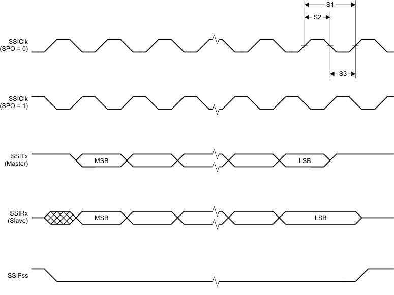
 Figure 7-3 SSI Timing for SPI Frame Format (FRF = 00), With SPH = 1