SLOSE70 December 2020 DRV8434S
PRODUCTION DATA
- 1 Features
- 2 Applications
- 3 Description
- 4 Revision History
- 5 Pin Configuration and Functions
- 6 Specifications
-
7 Detailed Description
- 7.1 Overview
- 7.2 Functional Block Diagram
- 7.3
Feature Description
- 7.3.1 Stepper Motor Driver Current Ratings
- 7.3.2 PWM Motor Drivers
- 7.3.3 Microstepping Indexer
- 7.3.4 Controlling VREF with an MCU DAC
- 7.3.5 Current Regulation
- 7.3.6
Decay Modes
- 7.3.6.1 Slow Decay for Increasing and Decreasing Current
- 7.3.6.2 Slow Decay for Increasing Current, Mixed Decay for Decreasing Current
- 7.3.6.3 Slow Decay for Increasing Current, Fast Decay for Decreasing current
- 7.3.6.4 Mixed Decay for Increasing and Decreasing Current
- 7.3.6.5 Smart tune Dynamic Decay
- 7.3.6.6 Smart tune Ripple Control
- 7.3.7 PWM OFF Time
- 7.3.8 Blanking time
- 7.3.9 Charge Pump
- 7.3.10 Linear Voltage Regulators
- 7.3.11 Logic Level, tri-level and quad-level Pin Diagrams
- 7.3.12 Protection Circuits
- 7.4 Device Functional Modes
- 7.5 Programming
- 7.6 Register Maps
- 8 Application and Implementation
- 9 Power Supply Recommendations
- 10Layout
- 11Device and Documentation Support
- 12Mechanical, Packaging, and Orderable Information
Package Options
Mechanical Data (Package|Pins)
Thermal pad, mechanical data (Package|Pins)
- RGE|24
Orderable Information
7.3.6 Decay Modes
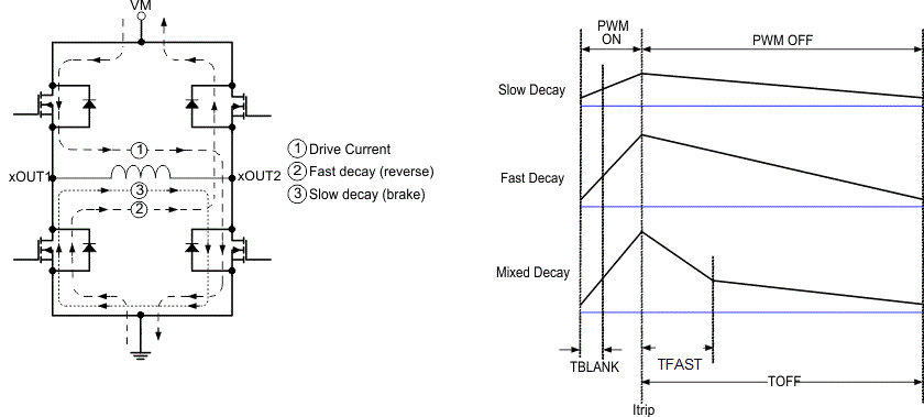
During PWM current chopping, the H-bridge is enabled to drive through the motor winding until the PWM current chopping threshold is reached. This is shown in Figure 7-6, Item 1.
Once the chopping current threshold is reached, the H-bridge can operate in two different states, fast decay or slow decay. In fast decay mode, as soon as the PWM chopping current level is reached, the H-bridge reverses state by switching on the opposite arm MOSFETs to allow the winding current to flow in the opposite direction. As the winding current approaches zero, the H-bridge is disabled to prevent further reverse current flow. Fast decay mode is shown in Figure 7-6, item 2. In slow decay mode, the winding current is re-circulated by enabling both low-side MOSFETs in the H-bridge. This is shown in Figure 7-6, Item 3.
 Figure 7-6 Decay Modes
The decay mode is selected by the DECAY register as shown in Table 7-7.
| DECAY | INCREASING STEPS | DECREASING STEPS |
|---|---|---|
| 000b | Slow decay | Slow decay |
| 001b | Slow decay | Mixed decay: 30% fast |
| 010b | Slow decay | Mixed decay: 60% fast |
| 011b | Slow decay | Fast decay |
| 100b | Mixed decay: 30% fast | Mixed decay: 30% fast |
| 101b | Mixed decay: 60% fast | Mixed decay: 60% fast |
| 110b | Smart tune Dynamic Decay | Smart tune Dynamic Decay |
| 111b (default) | Smart tune Ripple Control | Smart tune Ripple Control |
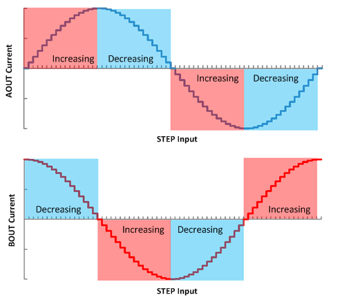
Figure 7-7 defines increasing and decreasing current. For the slow-mixed decay mode, the decay mode is set as slow during increasing current steps and mixed decay during decreasing current steps. In full step and noncircular 1/2-step operation, the decay mode corresponding to decreasing steps is always used.
 Figure 7-7 Definition of Increasing and Decreasing Steps