SLOSE70 December 2020 DRV8434S
PRODUCTION DATA
- 1 Features
- 2 Applications
- 3 Description
- 4 Revision History
- 5 Pin Configuration and Functions
- 6 Specifications
-
7 Detailed Description
- 7.1 Overview
- 7.2 Functional Block Diagram
- 7.3
Feature Description
- 7.3.1 Stepper Motor Driver Current Ratings
- 7.3.2 PWM Motor Drivers
- 7.3.3 Microstepping Indexer
- 7.3.4 Controlling VREF with an MCU DAC
- 7.3.5 Current Regulation
- 7.3.6
Decay Modes
- 7.3.6.1 Slow Decay for Increasing and Decreasing Current
- 7.3.6.2 Slow Decay for Increasing Current, Mixed Decay for Decreasing Current
- 7.3.6.3 Slow Decay for Increasing Current, Fast Decay for Decreasing current
- 7.3.6.4 Mixed Decay for Increasing and Decreasing Current
- 7.3.6.5 Smart tune Dynamic Decay
- 7.3.6.6 Smart tune Ripple Control
- 7.3.7 PWM OFF Time
- 7.3.8 Blanking time
- 7.3.9 Charge Pump
- 7.3.10 Linear Voltage Regulators
- 7.3.11 Logic Level, tri-level and quad-level Pin Diagrams
- 7.3.12 Protection Circuits
- 7.4 Device Functional Modes
- 7.5 Programming
- 7.6 Register Maps
- 8 Application and Implementation
- 9 Power Supply Recommendations
- 10Layout
- 11Device and Documentation Support
- 12Mechanical, Packaging, and Orderable Information
Package Options
Mechanical Data (Package|Pins)
Thermal pad, mechanical data (Package|Pins)
- RGE|24
Orderable Information
7.5.1.2 SPI for a Single Target Device
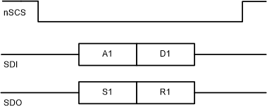
The SPI is used to set device configurations, operating parameters, and read out diagnostic information. The SPI operates in target mode. The SPI input-data (SDI) word consists of a 16-bit word, with 8 bits command and 8 bits of data. The SPI output data (SDO) word consists of 8 bits of status register with fault status indication and 8 bits of register data. Figure 7-23 shows the data sequence between the MCU and the SPI target driver.
 Figure 7-23 SPI Transaction Between MCU and the device
A valid frame must meet the following conditions:
- The SCLK pin must be low when the nSCS pin goes low and when the nSCS pin goes high.
- The nSCS pin should be taken high for at least 500 ns between frames.
- When the nSCS pin is asserted high, any signals at the SCLK and SDI pins are ignored, and the SDO pin is in the high-impedance state (Hi-Z).
- Full 16 SCLK cycles must occur.
- Data is captured on the falling edge of the clock and data is driven on the rising edge of the clock.
- The most-significant bit (MSB) is shifted in and out first.
- If the data word sent to SDI pin is less than 16 bits or more than 16 bits, a frame error occurs and the data word is ignored.
- For a write command, the existing data in the register being written to is shifted out on the SDO pin following the 8-bit command data.