SLOSE70 December 2020 DRV8434S
PRODUCTION DATA
- 1 Features
- 2 Applications
- 3 Description
- 4 Revision History
- 5 Pin Configuration and Functions
- 6 Specifications
-
7 Detailed Description
- 7.1 Overview
- 7.2 Functional Block Diagram
- 7.3
Feature Description
- 7.3.1 Stepper Motor Driver Current Ratings
- 7.3.2 PWM Motor Drivers
- 7.3.3 Microstepping Indexer
- 7.3.4 Controlling VREF with an MCU DAC
- 7.3.5 Current Regulation
- 7.3.6
Decay Modes
- 7.3.6.1 Slow Decay for Increasing and Decreasing Current
- 7.3.6.2 Slow Decay for Increasing Current, Mixed Decay for Decreasing Current
- 7.3.6.3 Slow Decay for Increasing Current, Fast Decay for Decreasing current
- 7.3.6.4 Mixed Decay for Increasing and Decreasing Current
- 7.3.6.5 Smart tune Dynamic Decay
- 7.3.6.6 Smart tune Ripple Control
- 7.3.7 PWM OFF Time
- 7.3.8 Blanking time
- 7.3.9 Charge Pump
- 7.3.10 Linear Voltage Regulators
- 7.3.11 Logic Level, tri-level and quad-level Pin Diagrams
- 7.3.12 Protection Circuits
- 7.4 Device Functional Modes
- 7.5 Programming
- 7.6 Register Maps
- 8 Application and Implementation
- 9 Power Supply Recommendations
- 10Layout
- 11Device and Documentation Support
- 12Mechanical, Packaging, and Orderable Information
Package Options
Mechanical Data (Package|Pins)
Thermal pad, mechanical data (Package|Pins)
- RGE|24
Orderable Information
7.3.6.6 Smart tune Ripple Control
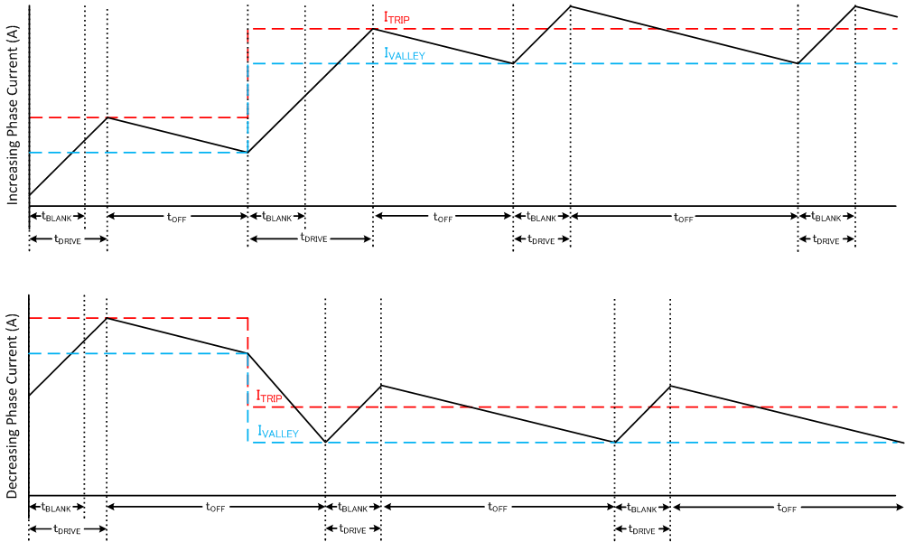
 Figure 7-13 Smart tune Ripple Control Decay Mode
Smart tune Ripple Control operates by setting an IVALLEY level along with the ITRIP level. When the current level reaches ITRIP, instead of entering slow decay until the tOFF time expires, the driver enters slow decay until IVALLEY is reached. Slow decay operates similar to slow/slow decay where both low-side MOSFETs are turned on allowing the current to recirculate. In this mode, tOFF is variable depending on the current level and operating parameters.
The ripple current in this decay mode is programmed by the RC_RIPPLE[1:0] bits. The ripple current is dependent on the ITRIP of a particular microstep level.
| RC_RIPPLE | Current Ripple at a specific microstep level |
|---|---|
| 00b | 19mA + 1% of ITRIP |
| 01b | 19mA + 2% of ITRIP |
| 10b | 19mA + 4% of ITRIP |
| 11b | 19mA + 6% of ITRIP |
This ripple control method allows much tighter regulation of the current level increasing motor efficiency and system performance. Smart tune Ripple Control can be used in systems that can tolerate a variable off-time regulation scheme to achieve low current ripple with current regulation. Select a lowest possible ripple current setting that ensures the PWM frequency is above the audible range.