SNOS641I October 1999 – July 2025 LM4041-N , LM4041-N-Q1
PRODUCTION DATA
- 1
- 1 Features
- 2 Applications
- 3 Description
- 4 Pin Configuration and Functions
-
5 Specifications
- 5.1 Absolute Maximum Ratings
- 5.2 ESD Ratings
- 5.3 Recommended Operating Conditions
- 5.4 Thermal Information
- 5.5 LM4041-N LM4041-N-Q1 1.2 Electrical Characteristics (Industrial Temperature Range)
- 5.6 LM4041-N LM4041-N-Q1 1.2 Electrical Characteristics (Industrial Temperature Range)
- 5.7 LM4041-N LM4041-N-Q1 1.2 Electrical Characteristics (Extended Temperature Range)
- 5.8 LM4041-N LM4041-N-Q1 ADJ (Adjustable) Electrical Characteristics (Industrial Temperature Range)
- 5.9 LM4041-N LM4041-N-Q1 ADJ (Adjustable) Electrical Characteristics (Extended Temperature Range)
- 5.10 Typical Characteristics
- 6 Parameter Measurement Information
- 7 Detailed Description
-
8 Application and Implementation
- 8.1 Application Information
- 8.2 Typical Applications
- 8.3 Power Supply Recommendations
- 8.4 Layout
- 9 Device and Documentation Support
- 10Revision History
- 11Mechanical, Packaging, and Orderable Information
Package Options
Mechanical Data (Package|Pins)
Thermal pad, mechanical data (Package|Pins)
Orderable Information
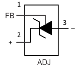
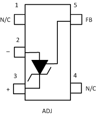
Pin Functions: ADJ Pinouts
 Figure 4-4 DBZ Package
3-Pin SOT-23
Top View
 Figure 4-5 DCK Package
5-Pin SC70
Top View
 Figure 4-6 LP Package
3-Pin TO-92
Bottom View
| PIN | I/O | DESCRIPTION | |||
|---|---|---|---|---|---|
| NAME | SOT-23 | SC70 | TO-92 | ||
| Anode | 3 | 2 | 3 | O | Anode pin, normally grounded |
| Cathode | 2 | 3 | 2 | I/O | Shunt current and output voltage |
| FB | 1 | 5 | 1 | I | Feedback pin for adjustable output voltage |
| NC** | — | — | — | — | **Must float or connect to anode |
| NC | — | 1, 4 | — | — | No connect |