SLOS224J July 1999 – February 2024 THS4031 , THS4032
PRODUCTION DATA
- 1
- 1 Features
- 2 Applications
- 3 Description
- 4 Pin Configuration and Functions
-
5 Specifications
- 5.1 Absolute Maximum Ratings
- 5.2 ESD Ratings
- 5.3 Recommended Operating Conditions
- 5.4 Thermal Information: THS4031
- 5.5 Thermal Information: THS4032
- 5.6 Electrical Characteristics: THS4031, RL = 150 Ω
- 5.7 Electrical Characteristics: THS4031, RL = 1 kΩ
- 5.8 Electrical Characteristics: THS4032, RL = 150 Ω
- 5.9 Electrical Characteristics: THS4032, RL = 1 kΩ
- 5.10 Typical Characteristics: THS4031
- 5.11 Typical Characteristics: THS4032
- 6 Detailed Description
- 7 Application and Implementation
- 8 Device and Documentation Support
- 9 Revision History
- 10Mechanical, Packaging, and Orderable Information
Package Options
Mechanical Data (Package|Pins)
Thermal pad, mechanical data (Package|Pins)
- DGN|8
Orderable Information
7.2 Typical Application
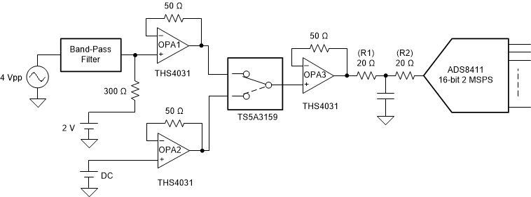
This section demonstrates multiplexing several analog input signals to a high-performance driver amplifier which subsequently drives a single high-resolution, high-speed SAR analog-to-digital converter (ADC). This example uses the ADS8411 and the TS5A3159 or TS5A3359 as the ADC and the multiplexer, respectively. This application uses the THS403x as the operational amplifier.
As detailed in Figure 7-4, the example system consists of an ADC (ADS8411), a driving operational amplifier (THS4031), a multiplexer (TS5A3159), an AC source, a DC source, and two driving operational amplifiers.
The driving amplifiers OPA1 are OPA2 are shown as two THS4031 amplifiers. Alternatively, use a single THS4032 to save on cost and board space. The purpose of these op-amps is make the input sources present a low impedance to rest of the circuit. Additionally, to maintain signal fidelity, these operational amplifiers must have low noise and distortion. The third THS4031 labeled OPA3 in Figure 7-4 is used to maintain switching speed and drive the ADC. The passive band-pass filter before the ADC reduces unwanted noise.
 Figure 7-4 Multiplexing Set-up to Drive a High Performance ADC