SBAU394B April   2022  – August 2025


  1.   1
  2.   Description
  3.   Features
  4.   4
  5. 1Evaluation Module Overview
    1. 1.1 Introduction
    2. 1.2 Kit Contents
    3. 1.3 Specification
    4. 1.4 Device Information
    5. 1.5 Quick Start Guide
  6. 2Hardware
    1. 2.1 ADC Analog Input Signal Path
    2. 2.2 ADC Connections and Decoupling
    3. 2.3 Power Supplies
    4. 2.4 ADC Input Clock (CLK) Options
    5. 2.5 Digital-to-Analog Converter (DAC)
    6. 2.6 Digital Interface
    7. 2.7 Connection to the PHI
    8. 2.8 Digital Header
  7. 3Software Installation
  8. 4EVM Configuration and GUI Operation
    1. 4.1 EVM Configuration
    2. 4.2 GUI Operation
      1. 4.2.1 EVM GUI Global Settings for ADC Control
      2. 4.2.2 Register Map Configuration Tool
      3. 4.2.3 Time Domain Display Tool
      4. 4.2.4 Spectral Analysis Tool
      5. 4.2.5 Histogram Tool
      6. 4.2.6 DAC Configuration Tool
  9. 5Hardware Design Files
    1. 5.1 Schematics
    2. 5.2 PCB Layout
    3. 5.3 Bill of Materials
  10. 6Additional Information
    1. 6.1 Trademarks
  11. 7References
  12. 8Revision History

PCB Layout

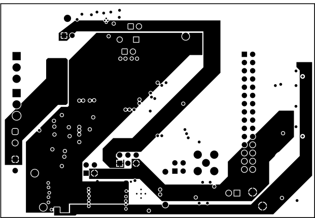
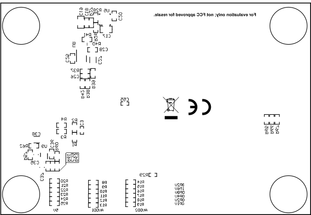
Figure 5-8 through Figure 5-13 show the ADS1285EVM-PDK PCB layout.

ADS1285EVM-PDK Top
                                                  SilkscreenFigure 5-8 Top Silkscreen
ADS1285EVM-PDK Ground Layer 1Figure 5-10 Ground Layer 1
ADS1285EVM-PDK Bottom LayerFigure 5-12 Bottom Layer
ADS1285EVM-PDK Top
                                                  LayerFigure 5-9 Top Layer
ADS1285EVM-PDK Power LayerFigure 5-11 Power Layer
ADS1285EVM-PDK Bottom SilkscreenFigure 5-13 Bottom Silkscreen