SLVAE87A December   2020  – October 2023 BQ79600-Q1 , BQ79612-Q1 , BQ79614-Q1 , BQ79616-Q1 , BQ79652-Q1 , BQ79654-Q1 , BQ79656-Q1


  1.   1
  2.   Abstract
  3.   Trademarks
  4. NPN LDO Supply
  5. AVDD, CVDD outputs and DVDD, NEG5, REFHP and REFHM
    1. 2.1 Base Device
    2. 2.2 Design Summary
  6. OTP Programming
  7. Cell Voltage Sense (VCn) and Cell Balancing (CBn)
    1. 4.1 Cell Voltage Sense (VCn)
    2. 4.2 Cell Balancing (CBn)
      1. 4.2.1 Non-Adjacent Cell Balancing
      2. 4.2.2 Adjacent Cell Balancing
      3. 4.2.3 Cell Balancing With External FET
    3. 4.3 Using Fewer Than 16 Cells
      1. 4.3.1 Design Summary
  8. Bus Bar Support
    1. 5.1 Bus Bar on BBP/BBN
    2. 5.2 Typical Connection
      1. 5.2.1 Cell Balancing Handling
    3. 5.3 Bus Bar on Individual VC Channel
    4. 5.4 Multiple Bus Bar Connections
      1. 5.4.1 Two Bus Bar Connections to One Device
      2. 5.4.2 Three Bus Bar Connections to One Device
      3. 5.4.3 Cell Balancing Handling
  9. TSREF
  10. General Purpose Input-Output (GPIO) Configurations
    1. 7.1 Ratiometric Temperature Measurement
    2. 7.2 SPI Mode
      1. 7.2.1 Support 8 NTC Thermistors With SPI Slave Device
      2. 7.2.2 Design Summary
  11. Base and Bridge Device Configuration
    1. 8.1 Power Mode Pings and Tones
      1. 8.1.1 Power Mode Pings
      2. 8.1.2 Power Mode Tones
      3. 8.1.3 Ping and Tone Propagation
    2. 8.2 UART Physical Layer
      1. 8.2.1 Design Considerations
  12. Daisy-Chain Stack Configuration
    1. 9.1 Communication Line Isolation
      1. 9.1.1 Capacitor Only Isolation
      2. 9.1.2 Capacitor and Choke Isolation
      3. 9.1.3 Transformer Isolation
      4. 9.1.4 Design Summary
    2. 9.2 Ring Communication
    3. 9.3 Re-Clocking
      1. 9.3.1 Design Summary
  13. 10Multi-Drop Configuration
  14. 11Main ADC Digital LPF
  15. 12AUX Anti Aliasing Filter (AAF)
  16. 13Layout Guidelines
    1. 13.1 Ground Planes
    2. 13.2 Bypass Capacitors for Power Supplies and References
    3. 13.3 Cell Voltage Sensing
    4. 13.4 Daisy Chain Communication
  17. 14BCI Performance
  18. 15Common and Differential Mode Noise
    1. 15.1 Design Consideration
  19. 16Revision History

Power Mode Pings

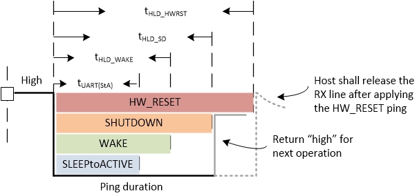
A ping is a specific high-low-high signal sent from MCU to the base device through the RX pin. Pings are used on the base device as only the base device is connected to the host from which the UART RX is accessible. The device detects the low pulse duration of the ping to differentiate between the different pings. There are total of 4 different pings as shown in Figure 8-3.

  • a WAKE ping through RX pin
  • a SHUTDOWN ping through RX pin
  • a SLEEPtoACTIVE ping through RX pin
  • a HW_RESET ping through RX pin
GUID-3506EE6B-719C-4C66-82CC-161484D3FBEA-low.jpg Figure 8-3 Communication Pings