SLVAE87A December 2020 – October 2023 BQ79600-Q1 , BQ79612-Q1 , BQ79614-Q1 , BQ79616-Q1 , BQ79652-Q1 , BQ79654-Q1 , BQ79656-Q1
- 1
- Abstract
- Trademarks
- 1 NPN LDO Supply
- 2 AVDD, CVDD outputs and DVDD, NEG5, REFHP and REFHM
- 3 OTP Programming
- 4 Cell Voltage Sense (VCn) and Cell Balancing (CBn)
- 5 Bus Bar Support
- 6 TSREF
- 7 General Purpose Input-Output (GPIO) Configurations
- 8 Base and Bridge Device Configuration
- 9 Daisy-Chain Stack Configuration
- 10Multi-Drop Configuration
- 11Main ADC Digital LPF
- 12AUX Anti Aliasing Filter (AAF)
- 13Layout Guidelines
- 14BCI Performance
- 15Common and Differential Mode Noise
- 16Revision History
1 NPN LDO Supply
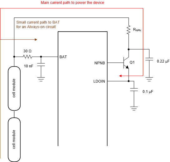
The device is powered by BAT pin and the LDOIN pin, with which the LDOIN pin is regulated by the pre- regulation circuit form with an external NPN. The device can be powered by a battery module with as low as 9V (without OTP programming) on the BAT pin.
The BAT and LDOIN pins should be filtered separately from the cell. This is to protect against hotplug, in-rush current, and other relevant noise. Recommended filters are RBAT = 30 Ω / .25 W, CBAT = 0.01 µF / 100 V for the BAT pin, two resistors in series for best thermal performance: RNPNC1 = 100 Ω / .75W, RNPNC2 = 200 Ω / .75 W and capacitor CNPNC = 0.22 µF / 100 V for the collector. LDOIN is the input for the external LDO supply for the BQ79616-Q1. Figure 1-1 shows the typical circuit.
 Figure 1-1 Power Supply Schematic
The resistor values and NPN can be further optimized from the reference schematic values based on the min and max module voltages for different projects.
Select the NPN Transistor based on the following criteria:
- Collector-Emitter Breakdown Voltage (BVCEO) > 80- 100 V (or the module voltage, plus any derating)
- DC gain (β, or approximately equal to hfe (AC gain)) > 80 at the expected load current
- Collector-based capacitance < 35 pF at typical base-voltage range
- Power handling ≥ 1 W
- Current handling > 100 mA
The resistor RNPNB in Figure 1-1 serves several purposes:
- Limits inrush current
- Shares some power dissipation away from the NPN transistor
- Combine with the CNPN to serve as a filter
where
- VBAT(min) is minimum battery module voltage which depends on the number of cells in series and minimum voltage per cell
- VCE(SAT) = VCE min at VBE(on), from transistor data sheet
- ILOAD is inrush current during startup or maximum active current and any external loading on CVDD
Connect the filter on the LDOIN supply (CLDOIN ) for stability. Use CLDOIN = 0.1 µF with a voltage rating of 10 V.