SLVAE87A December   2020  – October 2023 BQ79600-Q1 , BQ79612-Q1 , BQ79614-Q1 , BQ79616-Q1 , BQ79652-Q1 , BQ79654-Q1 , BQ79656-Q1


  1.   1
  2.   Abstract
  3.   Trademarks
  4. NPN LDO Supply
  5. AVDD, CVDD outputs and DVDD, NEG5, REFHP and REFHM
    1. 2.1 Base Device
    2. 2.2 Design Summary
  6. OTP Programming
  7. Cell Voltage Sense (VCn) and Cell Balancing (CBn)
    1. 4.1 Cell Voltage Sense (VCn)
    2. 4.2 Cell Balancing (CBn)
      1. 4.2.1 Non-Adjacent Cell Balancing
      2. 4.2.2 Adjacent Cell Balancing
      3. 4.2.3 Cell Balancing With External FET
    3. 4.3 Using Fewer Than 16 Cells
      1. 4.3.1 Design Summary
  8. Bus Bar Support
    1. 5.1 Bus Bar on BBP/BBN
    2. 5.2 Typical Connection
      1. 5.2.1 Cell Balancing Handling
    3. 5.3 Bus Bar on Individual VC Channel
    4. 5.4 Multiple Bus Bar Connections
      1. 5.4.1 Two Bus Bar Connections to One Device
      2. 5.4.2 Three Bus Bar Connections to One Device
      3. 5.4.3 Cell Balancing Handling
  9. TSREF
  10. General Purpose Input-Output (GPIO) Configurations
    1. 7.1 Ratiometric Temperature Measurement
    2. 7.2 SPI Mode
      1. 7.2.1 Support 8 NTC Thermistors With SPI Slave Device
      2. 7.2.2 Design Summary
  11. Base and Bridge Device Configuration
    1. 8.1 Power Mode Pings and Tones
      1. 8.1.1 Power Mode Pings
      2. 8.1.2 Power Mode Tones
      3. 8.1.3 Ping and Tone Propagation
    2. 8.2 UART Physical Layer
      1. 8.2.1 Design Considerations
  12. Daisy-Chain Stack Configuration
    1. 9.1 Communication Line Isolation
      1. 9.1.1 Capacitor Only Isolation
      2. 9.1.2 Capacitor and Choke Isolation
      3. 9.1.3 Transformer Isolation
      4. 9.1.4 Design Summary
    2. 9.2 Ring Communication
    3. 9.3 Re-Clocking
      1. 9.3.1 Design Summary
  13. 10Multi-Drop Configuration
  14. 11Main ADC Digital LPF
  15. 12AUX Anti Aliasing Filter (AAF)
  16. 13Layout Guidelines
    1. 13.1 Ground Planes
    2. 13.2 Bypass Capacitors for Power Supplies and References
    3. 13.3 Cell Voltage Sensing
    4. 13.4 Daisy Chain Communication
  17. 14BCI Performance
  18. 15Common and Differential Mode Noise
    1. 15.1 Design Consideration
  19. 16Revision History

Cell Voltage Sense (VCn)

The VCn pins are the primary inputs for measuring the cell voltages. VC0 is the low side reference to the negative terminal of the bottom cell and VC16 is the high side reference to the positive terminal of the top cell.

The inputs should be connected to the cells using series resistors to limit current into the pins and protect the IC from system transients. When fewer than 16 cells are used on the BQ79616-Q1, the lower cells must be used in order. Unused cell connections can be found in the scenarios shown in Figure 4-1.

Recommended filter capacitor for VCn pins is 0.47 μF/16 V.

A 100 Ω is recommended as a series filter resistor for VCn pins. A 100 Ω is an optimized value to protect VCn pins from hotplug and provide better filtering. But if another value is considered other than 100 Ω, it should be simulated for selecting the optimized value for the system.
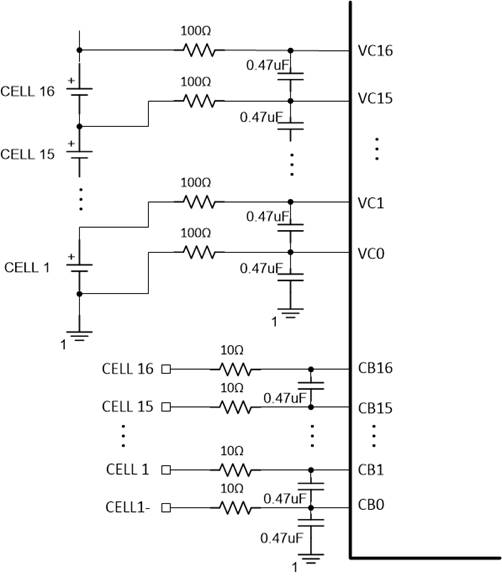
GUID-53D6BACE-8CF5-4C1D-9D65-C7F1BD8A3143-low.jpg
Note: New recommendation to add 470 nF/16 V from CB16 to BAT for hotplug robustness not shown in figure, see data sheet for details.
Figure 4-1 Cell Voltage Monitoring