SLVAE87A December 2020 – October 2023 BQ79600-Q1 , BQ79612-Q1 , BQ79614-Q1 , BQ79616-Q1 , BQ79652-Q1 , BQ79654-Q1 , BQ79656-Q1
- 1
- Abstract
- Trademarks
- 1 NPN LDO Supply
- 2 AVDD, CVDD outputs and DVDD, NEG5, REFHP and REFHM
- 3 OTP Programming
- 4 Cell Voltage Sense (VCn) and Cell Balancing (CBn)
- 5 Bus Bar Support
- 6 TSREF
- 7 General Purpose Input-Output (GPIO) Configurations
- 8 Base and Bridge Device Configuration
- 9 Daisy-Chain Stack Configuration
- 10Multi-Drop Configuration
- 11Main ADC Digital LPF
- 12AUX Anti Aliasing Filter (AAF)
- 13Layout Guidelines
- 14BCI Performance
- 15Common and Differential Mode Noise
- 16Revision History
13.1 Ground Planes
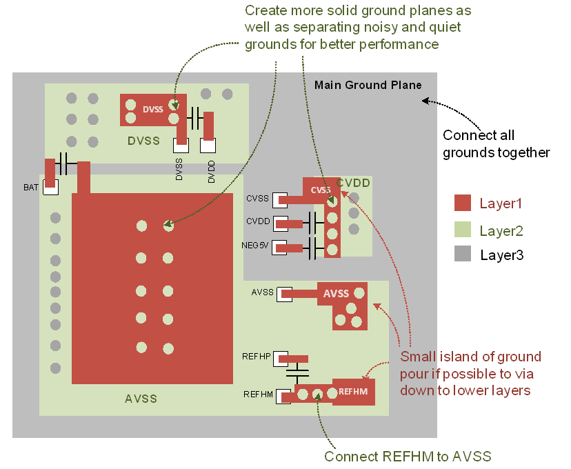
It is very important to establish a clean grounding scheme to ensure best performance of the device. There are 3 ground pins (AVSS, DVSS, CVSS) for the device’s internal power supplies and 1 ground reference (REFHM) for the precision reference. There are noisy grounds and quiet grounds that shall be separated in the layout initially and re-joint together in a lower PCB layer. The external components (e.g. bypass capacitors) shall be tied to the proper grounding group if possible to keep the separation of noisy and quiet grounds apart.
- AVSS ground:
- Bypass capacitor for these pins: BAT, VC0, CB0, LDOIN, TSREF
- Package lower pad
- DVSS ground:
- Bypass capacitor for DVDD
- GPIO filter capacitor (if used). It can also connect to AVSS ground plane if needed
- CVSS ground:
- Bypass capacitor for CVDD
- The bypass capacitors for COMHP/N and COMLP/N
- REFHM ground:
- Bypass capacitor for REFHP
- If possible, separate out REFHM from AVSS on the signal connection layer and reconnect REFHM to the AVSS ground plane on a lower layer
Even on a PCB layer that is mainly for signal routing, it is good practice to have as small an island of ground pour as possible to provide a low impedance ground, rather than simply via down the ground trace to an lower ground plane.

There is a strong recommendation to have a minimum of four layers in the PCB, with one fully dedicated as an unbroken VSS plane (except thermal reliefs). Avoid placing tracks on this layer to maintain the unbroken integrity of the plane structure.
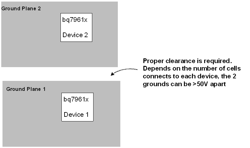
If multiple devices are placed on the same PCB, each device should have its own ground plane with proper layout clearance.
 Figure 13-2 Separate Ground Plane per
Device on the Same PCB