SLVAE87A December 2020 – October 2023 BQ79600-Q1 , BQ79612-Q1 , BQ79614-Q1 , BQ79616-Q1 , BQ79652-Q1 , BQ79654-Q1 , BQ79656-Q1
- 1
- Abstract
- Trademarks
- 1 NPN LDO Supply
- 2 AVDD, CVDD outputs and DVDD, NEG5, REFHP and REFHM
- 3 OTP Programming
- 4 Cell Voltage Sense (VCn) and Cell Balancing (CBn)
- 5 Bus Bar Support
- 6 TSREF
- 7 General Purpose Input-Output (GPIO) Configurations
- 8 Base and Bridge Device Configuration
- 9 Daisy-Chain Stack Configuration
- 10Multi-Drop Configuration
- 11Main ADC Digital LPF
- 12AUX Anti Aliasing Filter (AAF)
- 13Layout Guidelines
- 14BCI Performance
- 15Common and Differential Mode Noise
- 16Revision History
4.2.1 Non-Adjacent Cell Balancing
Auto balancing control is configured by setting [AUTO_BAL] = 1. In auto balancing control mode, CBFETs are enabled in an odd and even sequence.
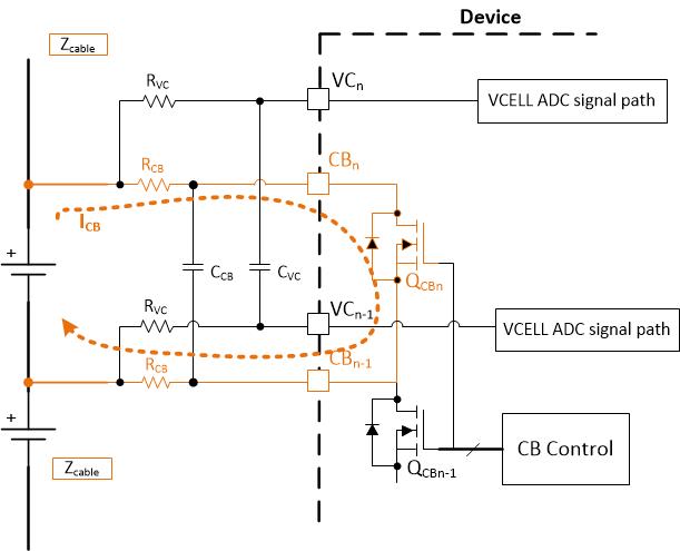
 Figure 4-2 Internal CB Diagram (no
adjacent cell balancing)
Figure 4-2 Internal CB Diagram (no
adjacent cell balancing)Figure 4-2 shows the cell balancing current path. Cell balancing current (ICB ) is dependent on cell voltage (VCELL) and the resistance of the balancing path (2 × RCB+ RDS(ON)). The equation is shown in Equation 2. RCB is the series resistor. RDS(ON) is the resistance of the internal FET when it is on. The higher the total resistance of the path, the lower the cell balancing current that flows.
To get a target cell balancing current, RCB can be chosen by following two steps.
Step 1 : Select RCB value
The RCB value can be calculated considering the desired cell balancing current at the highest RDS(ON) at the highest operating temperature using the equation in Equation 3.
Step 2 : Calculate RCB power rating
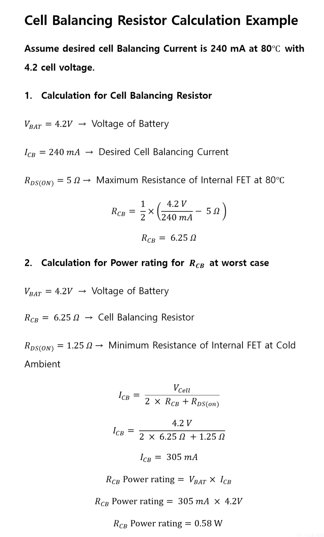
Power rating for RCB can be calculated with the highest cell balancing current at the minimum RDS(ON). An example calculation for how to select the value of RCB and power rating to get the desired cell balancing current is shown in Figure 4-3.
 Figure 4-3 Cell Balancing Resistor
Example Calculation
Figure 4-3 Cell Balancing Resistor
Example CalculationPassive balancing dissipates heat to the die, increasing the die temperature as balancing current increases. Refer to the BQ79616-Q1 data sheet for the recommended maximum balancing current according to the ambient temperature.