SLVAE87A December   2020  – October 2023 BQ79600-Q1 , BQ79612-Q1 , BQ79614-Q1 , BQ79616-Q1 , BQ79652-Q1 , BQ79654-Q1 , BQ79656-Q1


  1.   1
  2.   Abstract
  3.   Trademarks
  4. NPN LDO Supply
  5. AVDD, CVDD outputs and DVDD, NEG5, REFHP and REFHM
    1. 2.1 Base Device
    2. 2.2 Design Summary
  6. OTP Programming
  7. Cell Voltage Sense (VCn) and Cell Balancing (CBn)
    1. 4.1 Cell Voltage Sense (VCn)
    2. 4.2 Cell Balancing (CBn)
      1. 4.2.1 Non-Adjacent Cell Balancing
      2. 4.2.2 Adjacent Cell Balancing
      3. 4.2.3 Cell Balancing With External FET
    3. 4.3 Using Fewer Than 16 Cells
      1. 4.3.1 Design Summary
  8. Bus Bar Support
    1. 5.1 Bus Bar on BBP/BBN
    2. 5.2 Typical Connection
      1. 5.2.1 Cell Balancing Handling
    3. 5.3 Bus Bar on Individual VC Channel
    4. 5.4 Multiple Bus Bar Connections
      1. 5.4.1 Two Bus Bar Connections to One Device
      2. 5.4.2 Three Bus Bar Connections to One Device
      3. 5.4.3 Cell Balancing Handling
  9. TSREF
  10. General Purpose Input-Output (GPIO) Configurations
    1. 7.1 Ratiometric Temperature Measurement
    2. 7.2 SPI Mode
      1. 7.2.1 Support 8 NTC Thermistors With SPI Slave Device
      2. 7.2.2 Design Summary
  11. Base and Bridge Device Configuration
    1. 8.1 Power Mode Pings and Tones
      1. 8.1.1 Power Mode Pings
      2. 8.1.2 Power Mode Tones
      3. 8.1.3 Ping and Tone Propagation
    2. 8.2 UART Physical Layer
      1. 8.2.1 Design Considerations
  12. Daisy-Chain Stack Configuration
    1. 9.1 Communication Line Isolation
      1. 9.1.1 Capacitor Only Isolation
      2. 9.1.2 Capacitor and Choke Isolation
      3. 9.1.3 Transformer Isolation
      4. 9.1.4 Design Summary
    2. 9.2 Ring Communication
    3. 9.3 Re-Clocking
      1. 9.3.1 Design Summary
  13. 10Multi-Drop Configuration
  14. 11Main ADC Digital LPF
  15. 12AUX Anti Aliasing Filter (AAF)
  16. 13Layout Guidelines
    1. 13.1 Ground Planes
    2. 13.2 Bypass Capacitors for Power Supplies and References
    3. 13.3 Cell Voltage Sensing
    4. 13.4 Daisy Chain Communication
  17. 14BCI Performance
  18. 15Common and Differential Mode Noise
    1. 15.1 Design Consideration
  19. 16Revision History

Adjacent Cell Balancing

Manual balancing control is configured by setting [AUTO_BAL] = 0. In manual balancing control mode, the host can enable two consecutive CBFETs, and a maximum of eight total CBFETs can be enabled (see Figure 4-4).

However, when two adjacent channels are enabled, the balancing current is twice as high or higher than the non-adjacent channel balancing current. The system designer shall take this into account if adjacent cell balancing is used. See Equation 4 to select the right adjacent cell balancing series resistor (RCB).
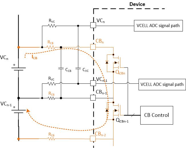
GUID-CFA0506D-ABA2-4C06-BBB8-AD494AA609A1-low.jpg Figure 4-4 Adjacent Cell Balancing
Equation 4. I C B   = 2   ×   V C n 2   × R C B   +   R d s o n Q C B n   +   R d s o n Q C B n - 1