SLVAE87A December 2020 – October 2023 BQ79600-Q1 , BQ79612-Q1 , BQ79614-Q1 , BQ79616-Q1 , BQ79652-Q1 , BQ79654-Q1 , BQ79656-Q1
- 1
- Abstract
- Trademarks
- 1 NPN LDO Supply
- 2 AVDD, CVDD outputs and DVDD, NEG5, REFHP and REFHM
- 3 OTP Programming
- 4 Cell Voltage Sense (VCn) and Cell Balancing (CBn)
- 5 Bus Bar Support
- 6 TSREF
- 7 General Purpose Input-Output (GPIO) Configurations
- 8 Base and Bridge Device Configuration
- 9 Daisy-Chain Stack Configuration
- 10Multi-Drop Configuration
- 11Main ADC Digital LPF
- 12AUX Anti Aliasing Filter (AAF)
- 13Layout Guidelines
- 14BCI Performance
- 15Common and Differential Mode Noise
- 16Revision History
4.2.3 Cell Balancing With External FET
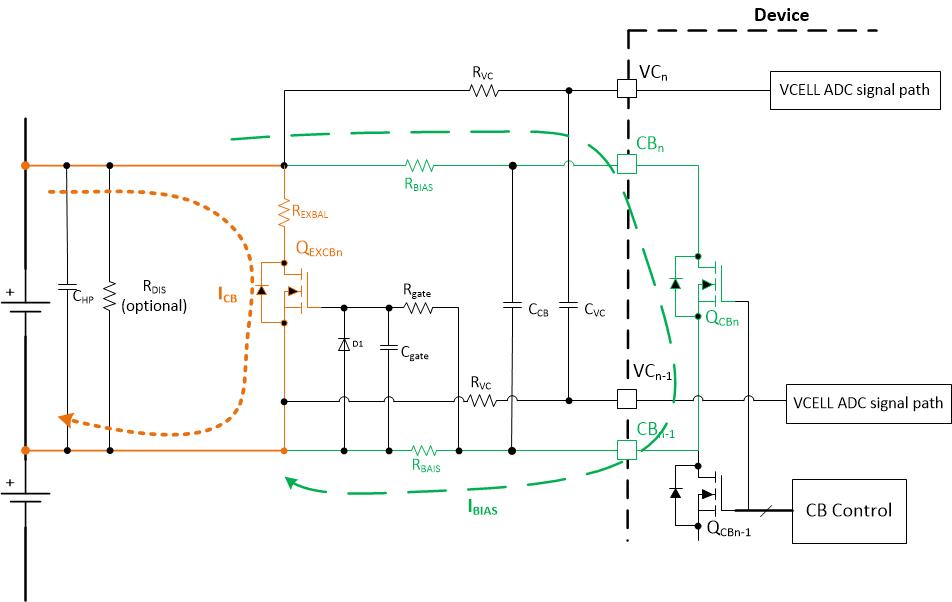
The BQ79616-Q1 can handle 240 mA max at 105°C. Should more current be needed, the cell balancing pins are able to support an external FET as shown in Figure 4-5. Cell balancing current with external FET can be calculated using equation below. Details for that configuration can be found in the BQ79616-Q1 data sheet.
There are a few things to keep in mind regarding external balancing. First, the series resistors between the FET and pin are there to protect the pins during hot plug and the capacitor is there to ensure that the FET does not turn on during hot plug. Also be aware of the following conditions that should be considered when selecting the FET.
- The VDS must be selected based on derating requirements determined by the stack voltage.
- The VGS threshold must be low enough to turn on with the lowest battery voltage planned for balancing. The gate of the MOSFET sees half of the battery voltage, so the VGS of the MOSFET must be selected to provide sufficiently low RDS(ON) at half of the lowest battery voltage.
 Figure 4-5 External FET Cell
Balancing