SLVAE87A December 2020 – October 2023 BQ79600-Q1 , BQ79612-Q1 , BQ79614-Q1 , BQ79616-Q1 , BQ79652-Q1 , BQ79654-Q1 , BQ79656-Q1
- 1
- Abstract
- Trademarks
- 1 NPN LDO Supply
- 2 AVDD, CVDD outputs and DVDD, NEG5, REFHP and REFHM
- 3 OTP Programming
- 4 Cell Voltage Sense (VCn) and Cell Balancing (CBn)
- 5 Bus Bar Support
- 6 TSREF
- 7 General Purpose Input-Output (GPIO) Configurations
- 8 Base and Bridge Device Configuration
- 9 Daisy-Chain Stack Configuration
- 10Multi-Drop Configuration
- 11Main ADC Digital LPF
- 12AUX Anti Aliasing Filter (AAF)
- 13Layout Guidelines
- 14BCI Performance
- 15Common and Differential Mode Noise
- 16Revision History
9 Daisy-Chain Stack Configuration
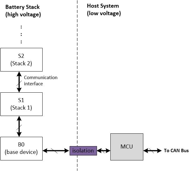
In the stacked configuration, the main microcontroller first communicates through a BQ79616-Q1 base device using the UART communications interface. Communication is then relayed up the chain of connected slave BQ79616-Q1 devices using a proprietary differential communications protocol over AC-coupled differential links interconnected by the COMMH± and COMML± pins. A high level diagram of this can be seen in Figure 9-1.
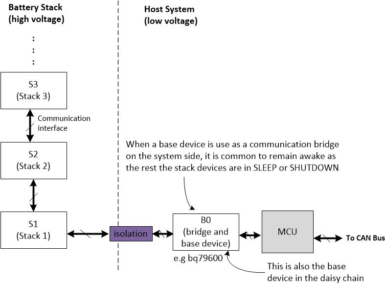
In the case of BQ79616 -Q1 working with a BQ79600-Q1 communication extender, the host microcontroller first communicates through a bridge device by UART or SPI. A command is then moved up the chain of connected slave BQ79616-Q1 devices through COML and COMH pins vertically as described in Figure 9-2.
 Figure 9-1 Daisy Chain Structure With a
Base Device
 Figure 9-2 Daisy Chain Structure With a
Bridge Device