SLVAE87A December 2020 – October 2023 BQ79600-Q1 , BQ79612-Q1 , BQ79614-Q1 , BQ79616-Q1 , BQ79652-Q1 , BQ79654-Q1 , BQ79656-Q1
- 1
- Abstract
- Trademarks
- 1 NPN LDO Supply
- 2 AVDD, CVDD outputs and DVDD, NEG5, REFHP and REFHM
- 3 OTP Programming
- 4 Cell Voltage Sense (VCn) and Cell Balancing (CBn)
- 5 Bus Bar Support
- 6 TSREF
- 7 General Purpose Input-Output (GPIO) Configurations
- 8 Base and Bridge Device Configuration
- 9 Daisy-Chain Stack Configuration
- 10Multi-Drop Configuration
- 11Main ADC Digital LPF
- 12AUX Anti Aliasing Filter (AAF)
- 13Layout Guidelines
- 14BCI Performance
- 15Common and Differential Mode Noise
- 16Revision History
9.1.1 Capacitor Only Isolation
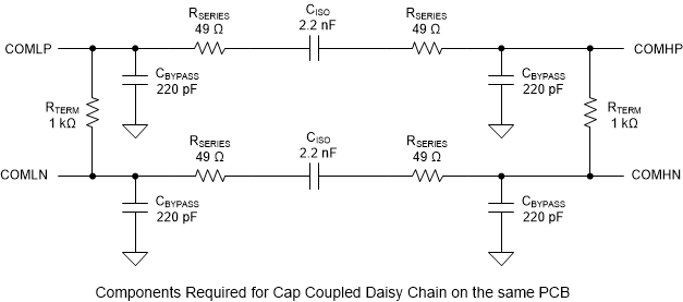
The first solution, capacitor isolation, is best suited for reducing noise and providing voltage isolation for ICs that are located on the same PCB. Figure 9-3 shows how this configuration would look for two ICs connected on the same PCB. A 10-kΩ termination resistor must be added at the high and low sides. In addition a 49-Ω resistor and 220-pF capacitor must be added on each line on both the high and low side to proved additional filtering. The capacitor must be 2.2 nF with a voltage rating twice that of the local cell stack. For example, for a 400-V system, a 800-V capacitor is needed. This configuration must be done on both the COMM± lines.
 Figure 9-3 Components Required for Cap
Coupled Daisy Chain in the Same PCB
Figure 9-3 Components Required for Cap
Coupled Daisy Chain in the Same PCBFigure 9-4 shows capacitive coupling isolation between two separated PCB. The capacitor needs to be 2.2 nF with a voltage range twice that of the local cell stack. One capacitor is sufficient, but if additional safety is needed then two can be used, one at each end of the cable. In this case a 220-pF capacitor must be used. Capacitance has a direct effect on performance, so all intended and parasitic capacitance must be taken into account when choosing components.
 Figure 9-4 Components Required for Cap
Coupled Daisy Chain in Different PCB