SLVAE87A December 2020 – October 2023 BQ79600-Q1 , BQ79612-Q1 , BQ79614-Q1 , BQ79616-Q1 , BQ79652-Q1 , BQ79654-Q1 , BQ79656-Q1
- 1
- Abstract
- Trademarks
- 1 NPN LDO Supply
- 2 AVDD, CVDD outputs and DVDD, NEG5, REFHP and REFHM
- 3 OTP Programming
- 4 Cell Voltage Sense (VCn) and Cell Balancing (CBn)
- 5 Bus Bar Support
- 6 TSREF
- 7 General Purpose Input-Output (GPIO) Configurations
- 8 Base and Bridge Device Configuration
- 9 Daisy-Chain Stack Configuration
- 10Multi-Drop Configuration
- 11Main ADC Digital LPF
- 12AUX Anti Aliasing Filter (AAF)
- 13Layout Guidelines
- 14BCI Performance
- 15Common and Differential Mode Noise
- 16Revision History
2.1 Base Device
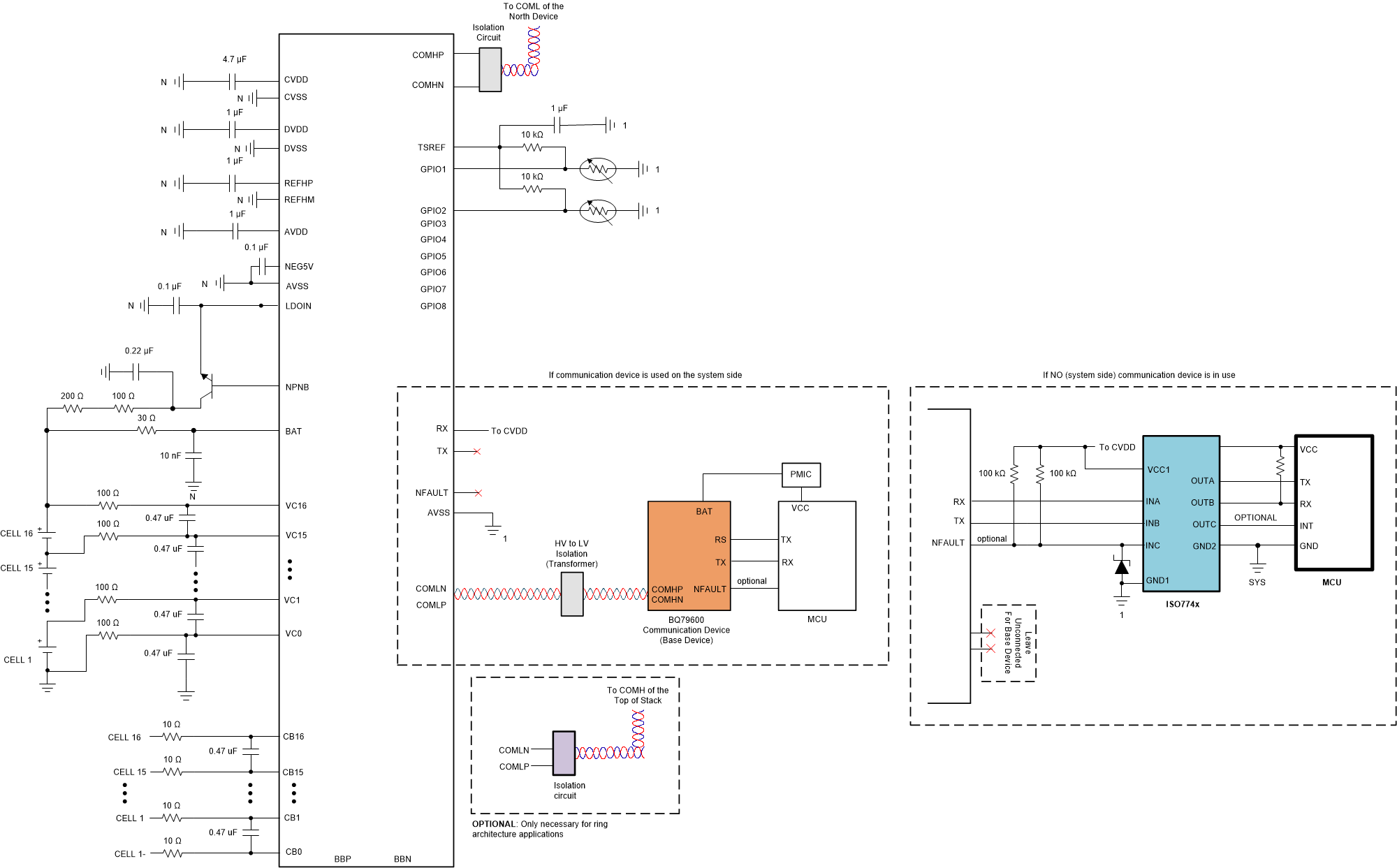
- AVDD is a 5-V regulated output which supplies internal circuits. AVDD must be bypassed to AVSS with a 1-µF/10-V capacitor. Do not connect any additional loads to AVDD.
- CVDD is a power supply for stack communication and tied to internally as I/O power supply. CVDD supplies the stack daisy chain communication transceiver circuit. Bypass CVDD with a 4.7 µF / 10 V and 100 nF and 22 nF for improved emissions and performance. capacitor to CVSS.
- DVDD is a 1.8-V regulated output that is used to power the digital logic inside the chip. Connect with a 1-μF/10-V capacitor to DVSS. Do not connect any additional loads to DVDD.
- NEG5V is a -5-V supply provided by an internal charge pump. Connect with a 0.1-µF/10-V capacitor to AVSS.
- REFHP is a precision reference output pin. A 1-µF/10-V bypass capacitor must be connected from REFHP to REFHM directly for proper operation of the part.
- REFHM is the precision reference ground for the internal precision reference. Connect DVSS, CVSS, ADC_AVSS, REFHM, and AVSS externally. All VSS pins must not be left unconnected.

Note: New recommendation to add 470
nF/16 V from CB16 to BAT for hotplug robustness not shown in figure, see data
sheet for details.
Figure 2-1 Regulator Connection for Base
Device