SLVAE87A December 2020 – October 2023 BQ79600-Q1 , BQ79612-Q1 , BQ79614-Q1 , BQ79616-Q1 , BQ79652-Q1 , BQ79654-Q1 , BQ79656-Q1
- 1
- Abstract
- Trademarks
- 1 NPN LDO Supply
- 2 AVDD, CVDD outputs and DVDD, NEG5, REFHP and REFHM
- 3 OTP Programming
- 4 Cell Voltage Sense (VCn) and Cell Balancing (CBn)
- 5 Bus Bar Support
- 6 TSREF
- 7 General Purpose Input-Output (GPIO) Configurations
- 8 Base and Bridge Device Configuration
- 9 Daisy-Chain Stack Configuration
- 10Multi-Drop Configuration
- 11Main ADC Digital LPF
- 12AUX Anti Aliasing Filter (AAF)
- 13Layout Guidelines
- 14BCI Performance
- 15Common and Differential Mode Noise
- 16Revision History
13.4 Daisy Chain Communication
Maintaining signal integrity while in a stacked configuration is critical to the success of this part. To maximize immunity from interfering signals, there are a couple design choices that need to be made. For transformer based communication, be sure to select a transformer that provides adequate isolation.
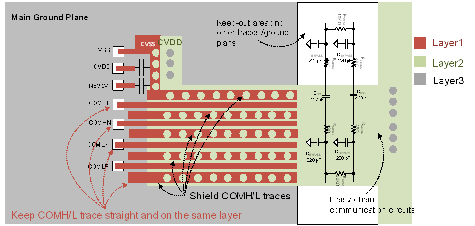
- Keep differential traces as short as possible and as straight as possible. Minimize turns and avoid any looping on the traces.
- Keep the differential traces on the same layers. Run the trace in parallel with shielding and matching trace impedance.
- Place the isolation components close to the connectors.
- When using capacitive isolation, place the high voltage capacitor of the COMxP/N pair (where x = H, L) close to each other along the parallel traces.
- Create a keep-out area (no other traces and no ground plane) around the daisy chain components in all PCB layers.

Note: The vias go through all 4
layers. Layer 4 is not shown as the bottom layer can include traces for any
bottom side components and a solid ground plane otherwise.
Figure 13-3 Daisy Chain Layout
Considerations