SPRACT2 August 2020 – MONTH AM67 , AM67 , AM67A , AM67A , AM68 , AM68 , AM68A , AM68A , AM69 , AM69 , AM69A , AM69A , DRA821U , DRA821U , DRA821U-Q1 , DRA821U-Q1 , DRA829J , DRA829J , DRA829J-Q1 , DRA829J-Q1 , DRA829V , DRA829V , DRA829V-Q1 , DRA829V-Q1 , TDA4AEN-Q1 , TDA4AEN-Q1 , TDA4AH-Q1 , TDA4AH-Q1 , TDA4AL-Q1 , TDA4AL-Q1 , TDA4AP-Q1 , TDA4AP-Q1 , TDA4APE-Q1 , TDA4APE-Q1 , TDA4VE-Q1 , TDA4VE-Q1 , TDA4VEN-Q1 , TDA4VEN-Q1 , TDA4VH-Q1 , TDA4VH-Q1 , TDA4VL-Q1 , TDA4VL-Q1 , TDA4VM , TDA4VM , TDA4VM-Q1 , TDA4VM-Q1 , TDA4VP-Q1 , TDA4VP-Q1 , TDA4VPE-Q1 , TDA4VPE-Q1
1 Introduction
Figure 1-1 shows the OSPI controller connected to the Flash device.
The data lines (DQ[7..0]) are bidirectional. During the command and address sections of the read transaction the controller drives those pins. During the data section of the transaction the flash devices drives the data lines. Figure 1-2 is an example of 4-byte read transaction.
 Figure 1-1 OSPI Controller and Flash
Device
Figure 1-1 OSPI Controller and Flash
DeviceThe controller provides the OSPI clock to the Flash device. It is generated by delaying the ref_clk through the TX PDL. The flash device uses the clock to capture the command and address during the command and address phases. During the data phase, the OSPI device drives a new data byte on each edge of the OSPI clock. Figure 1-2 is an example of 4-byte read transaction.
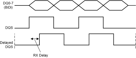
Some OSPI devices provide a DQS signal. The DQS and data are edge aligned at points 4 and 5 in Figure 1-1. DQS must be delayed by the RX PDL to a point inside the data eye to sample valid data at point 2.
 Figure 1-2 Timing Diagram of a Read
Transaction
Figure 1-2 Timing Diagram of a Read
TransactionThe “round trip delay” of data is the time from a ref_clk edge, to the sampling time of the data triggered by that edge. The sum of delays created by the TX PDL, the travel time of the OSPI clock from the controller to the flash device, the output delay of the flash device, and the RX PDL Delay, creates the round trip delay. The controller samples the data into an RX FIFO using the Delayed DQS. The data is read by the controller out of the RX FIFO using the ref_clk.
 Figure 1-3 Data Sampling
The controller expects the first byte of data to be captured within a specific ref_clk cycle (the target cycle), and all remaining data in the following cycles. In cases where the round trip delay is higher than the ref_clk period, the target cycle must be moved to the next ref_clk cycle using the Read Data Capture register’s Read Delay field OSPI_RD_DATA_CAPTURE_REG[4:1].
The goal of the tuning procedure is to select an optimal tuning point (OTP) of Read Delay, TX PDL Delay, and RX PDL Delay for sampling data.
 Figure 1-4 RCLK Target Cycles