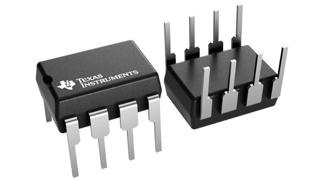
Packaging information
| Package | Pins PDIP (P) | 8 |
| Operating temperature range (°C) |
| Package qty | Carrier 50 | TUBE |
Features for the TLC2654
- Input Noise Voltage
0.5 uV (Peak-to-Peak) Typ, f = 0 to 1 Hz
1.5 uV (Peak-to-Peak) Typ, f = 0 to 10 Hz
47 nV/ Hz\ Typ, f = 10 Hz
13 nV/ Hz\ Typ, f = 1 kHz
 - High Chopping Frequency...10 kHz Typ
- No Clock Noise Below 10 kHz
- No Intermodulation Error Below 5 kHz
- Low Input Offset Voltage
10 uV Max (TLC2654A) - Excellent Offset Voltage Stability With Temperature...0.05 uV/°C Max
- AVD...135 dB Min (TLC2654A)
- CMRR...110 dB Min (TLC2654A)
- kSVR...110 dB Min
- Single-Supply Operation
- Common-Mode Input Voltage Range Includes the Negative Rail
- No Noise Degradation With External Capacitors Connected to VDD-
- Available in Q-Temp Automotive
HighRel Automotive Applications
Configuration Control/Print Support
Qualification to Automotive Standards
Advanced LinCMOS is a trademark of Texas Instruments.
Description for the TLC2654
The TLC2654 and TLC2654A are low-noise chopper-stabilized operational amplifiers using the Advanced LinCMOSTM process. Combining this process with chopper-stabilization circuitry makes excellent dc precision possible. In addition, circuit techniques are added that give the TLC2654 and TLC2654A superior noise performance.
Chopper-stabilization techniques provide for extremely high dc precision by continuously nulling input offset voltage even during variations in temperature, time, common-mode voltage, and power-supply voltage. The high chopping frequency of the TLC2654 and TLC2654A (see Figure 1) provides excellent noise performance in a frequency spectrum from near dc to 10 kHz. In addition, intermodulation or aliasing error is eliminated from frequencies up to 5 kHz.
This high dc precision and low noise, coupled with the extremely high input impedance of the CMOS input stage, makes the TLC2654 and TLC2654A ideal choices for a broad range of applications such as low-level, low-frequency thermocouple amplifiers and strain gauges and wide-bandwidth and subsonic circuits. For applications requiring even greater dc precision, use the TLC2652 or TLC2652A devices, which have a chopping frequency of 450 Hz.
The TLC2654 and TLC2654A common-mode input voltage range includes the negative rail, thereby providing superior performance in either single-supply or split-supply applications, even at power supply voltage levels as low as ±2.3 V.
Two external capacitors are required to operate the device; however, the on-chip chopper-control circuitry is transparent to the user. On devices in the 14-pin and 20-pin packages, the control circuitry is accessible, allowing the user the option of controlling the clock frequency with an external frequency source. In addition, the clock threshold of the TLC2554 and TLC2654A requires no level shifting when used in the single-supply configuration with a normal CMOS or TTL clock input.
Innovative circuit techniques used on the TLC2654 and TLC2654A allow exceptionally fast overload recovery time. An output clamp pin is available to reduce the recovery time even further.
The device inputs and outputs are designed to withstand -100-mA surge currents without
sustaining latch-up. In addition, the TLC2654 and TLC2654A incorporate internal ESD-protection circuits that prevent functional failures at voltages up to 2000 V as tested under MIL-STD-883C, Method 3015; however, exercise care in handling these devices, as exposure to ESD may result in degradation of the device parametric performance.
The C-suffix devices are characterized for operation from 0°C to 70°C. The I-suffix devices are characterized for operation from -40°C to 85°C. The Q-suffix devices are characterized for operation from -40°C to 125°C. The M-suffix devices are characterized for operation over the full military temperature range of -55°C to125°C.
