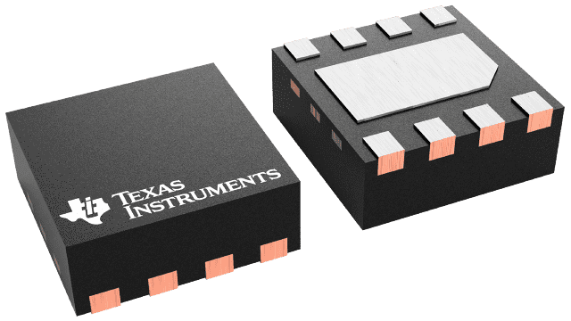
Gehäuseinformationen
| Gehäuse | Pins WSON (DSG) | 8 |
| Betriebstemperaturbereich (°C) -40 to 150 |
| Gehäusemenge | Träger 3.000 | LARGE T&R |
Merkmale von UCC27614
- Typical 10-A sink 10-A source output currents
- Input and enable pins capable of withstanding up to –10 V
- Absolute maximum VDD voltage: 30 V
- Wide VDD operating range from 4.5 V to 26 V with UVLO
- Available in 2-mm x 2-mm SON8 package
- Typical 17.5-ns propagation delay
- EN (enable) pin in SOIC8 package
- IN– pin can be used for enable/disable functionality
- VDD independent input thresholds (TTL compatible)
- Can be used as inverting or non-inverting driver
- Operating junction temperature range of –40°C to 150°C
Beschreibung von UCC27614
The UCC27614 is a single channel, high-speed, low-side gate driver capable of effectively driving MOSFET, IGBT, SiC, and GaN power switches. UCC27614 has a typical peak drive strength of 10 A, which reduces the rise and fall times of the power switches, lowering switching losses and increasing efficiency. The UCC27614 device’s small propagation delay yields better power stage efficiency by improving the dead-time optimization, pulse width utilization, control loop response, and transient performance of the system.
UCC27614 can handle –10-V on its inputs, which improves robustness in systems with moderate ground bouncing. The inputs are independent of supply voltage and can be connected to most controller outputs for maximum control flexibility. An independent enable signal allows the power stage to be controlled independent of the main control logic. The gate driver can quickly shut off the power stage if there is a fault in the system (which requires the power train to be turned-off). The enable function also improves system robustness. Many high-frequency switching power supplies exhibit high frequency noise at the gate of the power device, which can get injected into the output pin of the gate driver and can cause the driver to malfunction. The UCC27614 performs well in such conditions due to its transient reverse current and reverse voltage capability.
The strong internal pulldown MOSFET holds the output low if the VDD voltage is below the specified UVLO threshold. This active pulldown feature further improves system robustness. The UCC27614 device’s 10-A drive current in the 2-mm × 2mm package improves system power density. This small package also enables optimum gate driver placement and improved layout.