Inicio Interfaz Circuitos integrados LVDS, M-LVDS y PECL

SN55LVRA4-SEP

ACTIVO

Radiation-tolerant, Quad-channel high-speed differential receiver

Detalles del producto

Function Receiver Protocols LVDS Number of transmitters 0 Number of receivers 4 Signaling rate (Mbps) 400 Input signal CMOS, ECL, LVCMOS, LVDS, LVECL, LVPECL, PECL Output signal LVTTL Rating Space Operating temperature range (°C) -55 to 125
SOIC (D) 16 59.4 mm² (9.9 mm × 6 mm)
  • VID V62/25606-01XE
  • Total ionizing dose characterized at 30krad (Si)
    • Total ionizing dose radiation lot acceptance testing (TID RLAT) for every wafer lot to 30krad (Si)
  • Single-event effects (SEE) characterized:
    • Single event latch-up (SEL) immune to linear energy transfer (LET) = 50MeV-cm2 /mg
    • Single event transient (SET) characterization report available
  • 400Mbps signaling rate
  • Operates with a single 3.3V supply
  • –4V to 5V extended common-mode input voltage range
  • Differential input thresholds < ±50mV with 50mV of hysteresis over entire common-mode input voltage range
  • Complies with TIA/EIA-644 (LVDS)
  • Active fail-safe assures a high-level output with no input and input remains high-impedance on power down
  • Bus-pin ESD protection exceeds 15kV HBM
  • TTL control inputs are 5V tolerant
  • Space enhanced plastic (SEP)
    • Controlled baseline
    • Gold wire, NiPdAu lead finish
    • One assembly and test site, one fabrication site
    • Extended product life cycle
    • Military (–55°C to 125°C) temperature range
    • Product traceability
    • Meets NASA ASTM E595 outgassing specification
  • VID V62/25606-01XE
  • Total ionizing dose characterized at 30krad (Si)
    • Total ionizing dose radiation lot acceptance testing (TID RLAT) for every wafer lot to 30krad (Si)
  • Single-event effects (SEE) characterized:
    • Single event latch-up (SEL) immune to linear energy transfer (LET) = 50MeV-cm2 /mg
    • Single event transient (SET) characterization report available
  • 400Mbps signaling rate
  • Operates with a single 3.3V supply
  • –4V to 5V extended common-mode input voltage range
  • Differential input thresholds < ±50mV with 50mV of hysteresis over entire common-mode input voltage range
  • Complies with TIA/EIA-644 (LVDS)
  • Active fail-safe assures a high-level output with no input and input remains high-impedance on power down
  • Bus-pin ESD protection exceeds 15kV HBM
  • TTL control inputs are 5V tolerant
  • Space enhanced plastic (SEP)
    • Controlled baseline
    • Gold wire, NiPdAu lead finish
    • One assembly and test site, one fabrication site
    • Extended product life cycle
    • Military (–55°C to 125°C) temperature range
    • Product traceability
    • Meets NASA ASTM E595 outgassing specification

The SN55LVRA4-SEP offers the widest common-mode input voltage range in the industry. These receivers provide an input voltage range specification compatible with a 5V PECL signal as well as an overall increased ground-noise tolerance.

The SN55LVRA4-SEP include a failsafe circuit that provides a high-level output within 60ns after loss of the input signal. The most common causes of signal loss are disconnected cables, shorted lines, or powered-down transmitters. The failsafe circuit prevents noise from being received as valid data under these fault conditions.

The intended application and signaling technique of these devices is point-to-point baseband data transmission over controlled impedance media of approximately 100Ω. The transmission media can be printed-circuit board traces, backplanes, or cables. The ultimate rate and distance of data transfer is dependent upon the attenuation characteristics of the media and the noise coupling to the environment.

The SN55LVRA4-SEP is characterized for operation from –55°C to 125°C.
The SN55LVRA4-SEP offers the widest common-mode input voltage range in the industry. These receivers provide an input voltage range specification compatible with a 5V PECL signal as well as an overall increased ground-noise tolerance.

The SN55LVRA4-SEP include a failsafe circuit that provides a high-level output within 60ns after loss of the input signal. The most common causes of signal loss are disconnected cables, shorted lines, or powered-down transmitters. The failsafe circuit prevents noise from being received as valid data under these fault conditions.

The intended application and signaling technique of these devices is point-to-point baseband data transmission over controlled impedance media of approximately 100Ω. The transmission media can be printed-circuit board traces, backplanes, or cables. The ultimate rate and distance of data transfer is dependent upon the attenuation characteristics of the media and the noise coupling to the environment.

The SN55LVRA4-SEP is characterized for operation from –55°C to 125°C.

Descargar Ver vídeo con transcripción Video

Productos similares que pueden interesarle

open-in-new Comparar alternativas
Funcionalidad similar a la del dispositivo comparado
SN55LVTA4-SEP ACTIVO Radiation-tolerant, Quad-channel high-speed differential line driver Line Driver version

Documentación técnica

No se encontraron resultados. Borre su búsqueda y vuelva a intentarlo.
Ver todo 6
Documentación principal Tipo Título Opciones de formato Descargar la versión más reciente en inglés Fecha
* Hoja de datos SN55LVRA4-SEP Radiation Tolerant Quad Channel High-Speed Differential Receiver datasheet (Rev. B) PDF | HTML 19/02/2026
* Informe de radiación y confiabilidad SN55LVRA4-SEP Total Ionizing Dose (TID) Report 10/12/2025
* Informe de radiación y confiabilidad SN55LVRA4-SEP Single-Event Effects (SEE) Radiation Report PDF | HTML 8/12/2025
* Informe de radiación y confiabilidad SN55LVRA4-SEP Production Flow and Reliability Report PDF | HTML 12/11/2025
* VID SN55LVRA4-SEP VID SN55LVRA4-SEP VID V62-25606 20/02/2026
Guía de selección TI Space Products (Rev. L) 27/03/2026

Diseño y desarrollo

Para conocer los términos adicionales o los recursos necesarios, haga clic en cualquier título de abajo para ver la página de detalles cuando esté disponible.

Placa de evaluación

SN65LVDS31-33EVM — Módulo de evaluación para SN65LVDS31 y SN65LVDS33

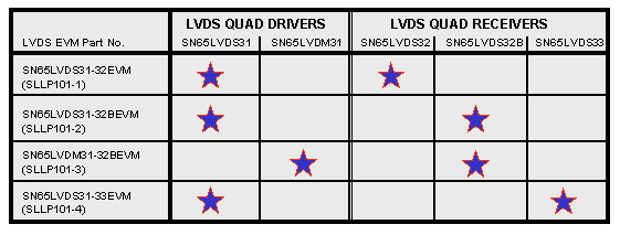
TI offers a series of low-voltage differential signaling (LVDS) evaluation modules (EVMs) designed for analysis of the electrical characteristics of LVDS drivers and receivers. Four unique EVMs are available to evaluate the different classes of LVDS devices offered by TI.

As seen in the Combination (...)

Productos y hardware compatibles
En inventario
Límite:
??asset.out-of-stock-ti_es_MX??
No disponible
Modelo de simulación

SN65LVDS33 IBIS Model (Rev. A)

SLLC069A.ZIP (6 KB) - Modelo IBIS
Productos y hardware compatibles
Encapsulado Pines Símbolos CAD, huellas y modelos 3D
SOIC (D) 16 Ultra Librarian

Pedidos y calidad

Los productos recomendados pueden tener parámetros, módulos de evaluación o diseños de referencia relacionados con este producto de TI.

Soporte y capacitación

Foros de TI E2E™ con asistencia técnica de los ingenieros de TI

El contenido lo proporcionan “tal como está” TI y los colaboradores de la comunidad y no constituye especificaciones de TI. Consulte los términos de uso.

Si tiene alguna pregunta sobre calidad, encapsulados o pedido de productos de TI, consulte el servicio de asistencia de TI. ​​​​​​​​​​​​​​

Videos