JAJU446A December 2017 – January 2022
- 概要
- Resources
- 特長
- アプリケーション
- 5
- 1 System Description
- 2 System Overview
- 3 Circuit Design
- 4 Host Interface
- 5 Hardware Functional Block
- 6 Getting Started Application GUI
- 7 Testing and Results
- 8 Design Files
- 9 Software Files
- 10Related Documentation
- 11About the Authors
- 12Revision History
2.4.4 Analog Front End
The front-end analog signal chain determines the performance in a multichannel receiver or data capture system, for which the SNR and SFDR are critical. The front-end gain and the attenuation block over the input signal bandwidth determine the overall system dynamic range.
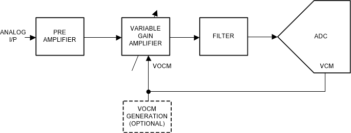
Figure 2-7 shows the typical AFE block for a high-speed digitizer and DSO. The front end contains a preamplifier, analog- or digital-variable gain amplifier (DVGA), and a multiple-order band-pass filter. The preamplifer and DVGA determine the system dynamic range and the filter improves the system harmonic distortion of a single-tone frequency. The signal chain SNR is designed such that it is greater than 10 dB of the ADC SNR.
 Figure 2-7 Typical AFE
Ensure that the front end is properly biased to achieve the ADC-rated performance at the full-scale input. The integrated buffer of the ADC has a common-mode bias output that the user can implement to directly drive the front-end amplifier without requiring an external circuit. The inputs of the unbuffered ADC require an external bias, which the designer can generate using various methods. This bias voltage is typically half of the supply voltage, so a simple resistor divider is enough to generate this external bias. See the relevant device data sheets for the recommended VCM generation guidelines.
A failure to maintain the common-mode voltage leads to ADC offset and gain error, which degrade the full-scale dynamic performance of the system.