JAJU446A December 2017 – January 2022
- 概要
- Resources
- 特長
- アプリケーション
- 5
- 1 System Description
- 2 System Overview
- 3 Circuit Design
- 4 Host Interface
- 5 Hardware Functional Block
- 6 Getting Started Application GUI
- 7 Testing and Results
- 8 Design Files
- 9 Software Files
- 10Related Documentation
- 11About the Authors
- 12Revision History
3.2 High-Speed Multichannel Clocking
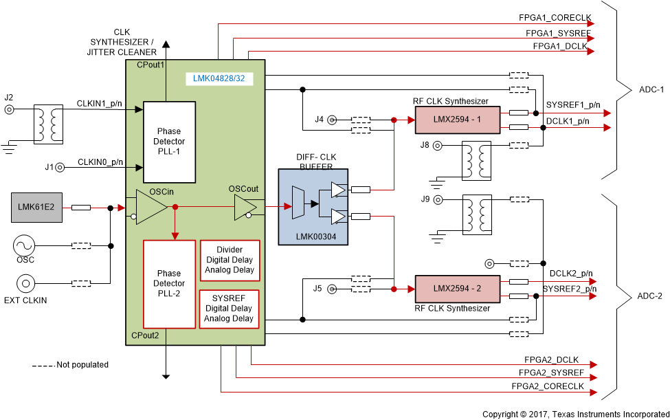
Figure 3-9 shows the clock tree of the TIDA-01022 design. The clock source is an essential component in signal chain design, specifically when driving the ADC sample clock. Clock jitter directly impacts ADC SNR performance and becomes proportionally greater at higher input signal frequencies. When clocking multiple channels, channel-to-channel skew is an important design consideration. Clock jitter and phase mismatch leads to deviation from the ideal sampling instant of a channel, which results in channel-to-channel skew. The LMX2594 synthesizers that this design uses have an excellent phase noise performance at high frequencies, which brings down the clock jitter to approximately 45 fs. Additionally, the phase synchronization feature of the LMX2594 helps to improve the channel-to-channel skew.
This flexible clocking platform helps the designer validate system performance with various input clock paths and sources. The TIDA-01022 design has three different clocking features to clock the ADC12DJ3200 device using any one of the clocking devices such as the LMK4828, LMX2594, and external clock input. In this design, the LMK4828 device is configured in distribution mode and generates the 33.75-MHz reference clock for the LMX2594 device and FPGA_SYSREF signal. The LMK4828 divider also generates 270-MHz FPGA clocks for FPGA DCLK, FPGA CORE CLK, and 33.75 MHz for the TSW14J56 capture card.
The output of the LMK4828 drives the clock buffer to distribute the reference to two LMX2594 devices, at which point both LMX devices are running in dual PLL mode to generate a low-phase noise clock of
2700 MHz for DEVCLK and a 33.75-MHz SYSREF for the ADC (ADC12DJ3200).
 Figure 3-9 TIDA-01022 Clock Tree